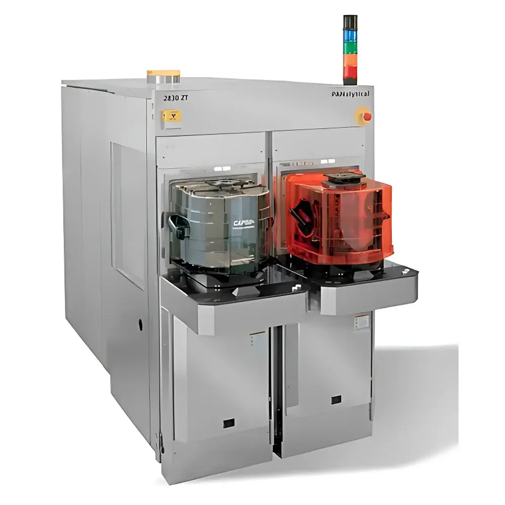
Malvern Panalytical 2830 ZT Wafer Analyzer
| Brand | Malvern Panalytical |
|---|---|
| Origin | Netherlands |
| Manufacturer Type | Original Equipment Manufacturer (OEM) |
| Origin Category | Imported |
| Model | 2830 ZT |
| Instrument Type | Floor-standing |
| X-ray Tube Power | 4 kW |
| Detector Configuration | Sequential Multi-channel |
| Analyzable Elements | B, C, N, O, F, Mg, TiSiₓ, CoSiₓ, WSiₓ |
Overview
The Malvern Panalytical 2830 ZT Wafer Analyzer is a high-performance, floor-standing Wavelength Dispersive X-ray Fluorescence (WDXRF) spectrometer engineered specifically for non-destructive metrology and compositional analysis of semiconductor wafers up to 300 mm in diameter. Utilizing Bragg diffraction principles with precisely calibrated analyzing crystals, the system delivers high spectral resolution and exceptional peak-to-background ratios—critical for quantifying thin-film thicknesses, layer stoichiometry, dopant concentrations, and lateral uniformity across full-wafer maps. Designed for integration into high-throughput semiconductor fabrication environments, the 2830 ZT operates under strict process control requirements while maintaining traceable measurement uncertainty consistent with ISO/IEC 17025 and ASTM E1361 standards for XRF-based thin-film characterization.
Key Features
- 4 kW SST-mAX X-ray source with patented ZETA (Zero-Emission Tube Aging) technology, eliminating tungsten filament evaporation and beryllium window contamination—ensuring stable tube output over its entire operational lifetime
- Reduced need for drift correction and recalibration cycles, enabling >95% instrument uptime and long-term measurement reproducibility (RSD < 0.8% for SiO₂/Si stack thickness at 2 nm)
- Dedicated wafer handling module FALMO-2G compliant with SEMI GEM300 standards; supports FOUP, SMIF, or open-cassette loading configurations with single- or dual-port options
- Optimized optical path geometry and high-efficiency Soller slits for enhanced light-element sensitivity (down to boron), critical for low-k dielectrics and ultra-thin barrier layers
- Robust mechanical design with active temperature stabilization and vibration-damped optical bench to maintain alignment integrity during extended mapping sequences
Sample Compatibility & Compliance
The 2830 ZT accommodates standard silicon, SOI, GaAs, and compound semiconductor wafers from 100 mm to 300 mm diameter, including patterned and unpatterned substrates. It supports both front-side and back-side analysis with automated surface height compensation. All hardware and software modules are designed to meet GLP/GMP documentation requirements, with audit-trail functionality compliant with FDA 21 CFR Part 11 for electronic records and signatures. Measurement protocols align with ASTM F2150 (standard test method for measuring thin film thickness by XRF) and ISO 14719 (XRF analysis of coated materials), ensuring regulatory acceptability in qualification and production release workflows.
Software & Data Management
Powered by SuperQ software suite, the 2830 ZT includes FP Multi—a physics-based fundamental parameters engine optimized for multi-layer thin-film systems. The interface supports fully automated recipe-driven analysis, including auto-focus, auto-alignment, and dynamic collimation selection per layer stack. Data export conforms to SECS/GEM and PVCS-compliant formats for seamless integration into factory MES and SPC platforms. Raw spectral data, calibration logs, and measurement reports are stored with time-stamped metadata and user-accessible revision history. Optional modules include statistical process monitoring (SPM), wafer map visualization (with color-coded uniformity overlays), and cross-tool correlation tools for inter-instrument comparability studies.
Applications
- Quantitative thickness and composition profiling of gate oxides, high-k dielectrics (e.g., HfO₂, Al₂O₃), metal gates (TiN, TaN), and silicide layers (TiSiₓ, CoSiₓ, WSiₓ)
- In-line process monitoring of ALD/CVD/PVD deposition uniformity and stoichiometric deviation across 300 mm wafers
- Failure analysis support for interfacial diffusion, oxidation state identification (e.g., Ti⁴⁺ vs Ti³⁺), and contamination screening (F, Na, K, Ca)
- Development and validation of new film stacks for advanced nodes (sub-5 nm logic, 3D NAND, DRAM scaling)
- Reference material certification and inter-laboratory round-robin studies requiring SI-traceable WDXRF measurements
FAQ
What is the minimum detectable thickness for SiO₂ on Si using the 2830 ZT?
For a 2 nm SiO₂/Si bilayer under standard measurement conditions (4 kW, LiF(200) crystal, 100 s counting time), the typical detection limit is ≤0.3 nm with RSD < 1.2%.
Does the system support automated wafer mapping with sub-millimeter spatial resolution?
Yes—the integrated motorized XY stage enables programmable raster scanning with positional repeatability of ±1.5 µm and configurable step sizes from 0.1 mm to 5 mm.
Can the 2830 ZT analyze elements lighter than sodium?
Yes—it routinely quantifies B, C, N, O, and F using vacuum-path optics and specialized crystals (e.g., LDE1, PET), with optimized excitation and background subtraction algorithms.
Is remote diagnostics and preventive maintenance supported?
Yes—via secure TLS-encrypted connection, the system provides real-time tube health monitoring, crystal aging diagnostics, and predictive alerts for consumables replacement (e.g., X-ray tube, detector gas, vacuum pump oil).