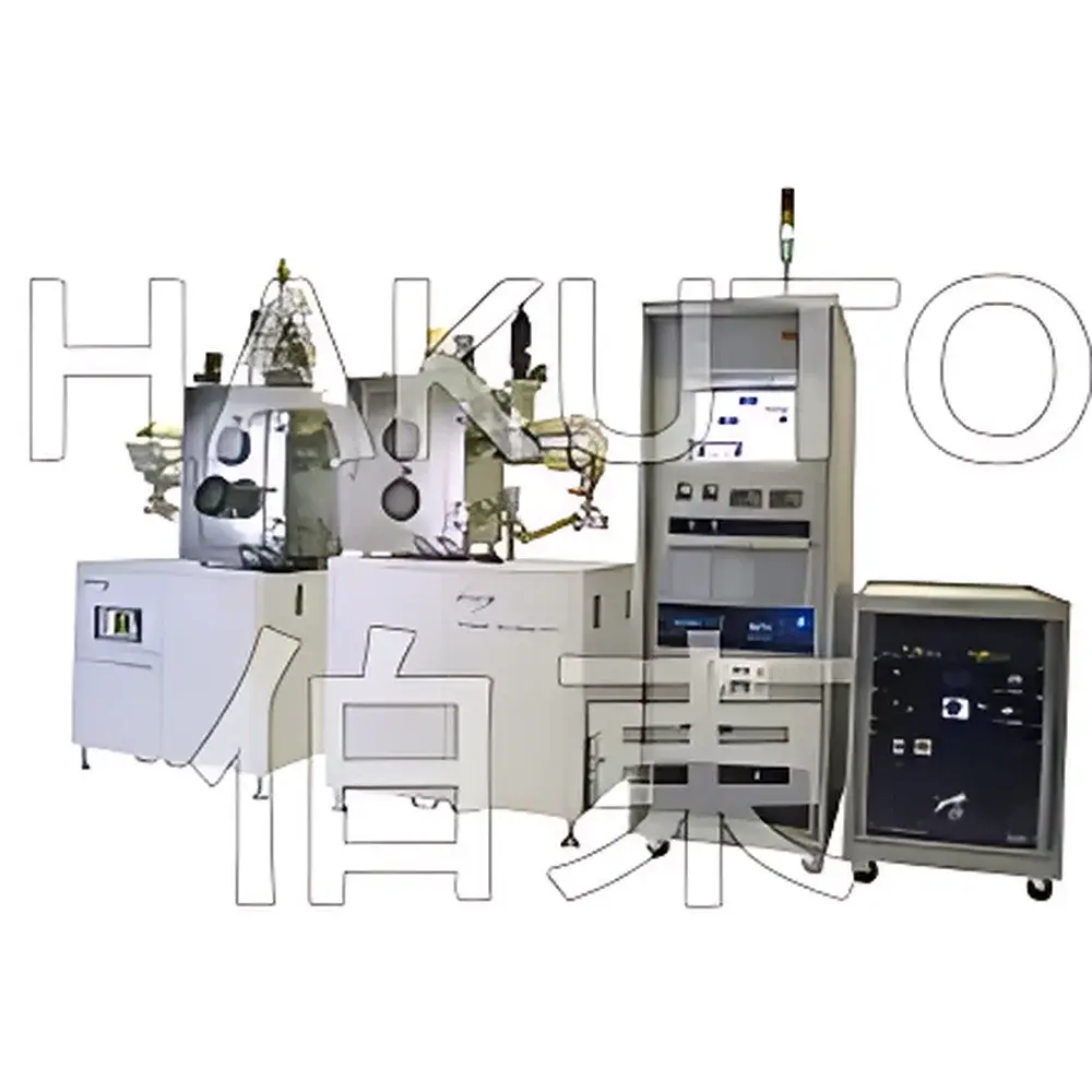
SYSKEY E-beam Evaporation System for Thin Film Deposition
| Brand | SYSKEY |
|---|---|
| Origin | Taiwan |
| Model | E-beam |
| Instrument Type | Electron Beam Evaporator |
| Substrate Size | Up to 12-inch wafer |
| Substrate Temperature Range | Ambient to 800 °C (heating) / Down to –70 °C (liquid nitrogen cooling) |
| Thickness Uniformity | ±3% |
| Base Pressure | ≤5×10⁻¹⁰ Torr (with cryopump) |
| Crucible Configuration | 1–6 water-cooled rotating crucibles (7–25 cc each) |
| Optional Integration | KRI ion source, load-lock, transfer chamber, glovebox, plasma cleaner |
Overview
The SYSKEY E-beam Evaporation System is an ultra-high-vacuum (UHV) physical vapor deposition (PVD) platform engineered for precision thin-film fabrication in semiconductor R&D, optoelectronics, and advanced materials science. Unlike thermal evaporation—limited by resistive heating constraints—the system employs focused electron beam bombardment to achieve localized temperatures exceeding 3000 °C, enabling reliable evaporation of high-melting-point materials including tungsten (W), molybdenum (Mo), tantalum (Ta), platinum (Pt), refractory oxides (e.g., ITO, Al₂O₃), and ceramic precursors. The system operates on the principle of electron kinetic energy conversion: a thermionically emitted electron beam is magnetically focused onto a solid target within a water-cooled crucible, inducing controlled volumetric heating without crucible contamination. This mechanism ensures high material utilization efficiency, minimal thermal stress on substrates, and exceptional stoichiometric fidelity for compound films. Designed for both research flexibility and pilot-scale reproducibility, the system supports single- or multi-wafer processing (up to 12-inch diameter), with base pressure reaching ≤5×10⁻¹⁰ Torr when equipped with a cryogenic pump—meeting stringent UHV requirements for low-defect-density film growth.
Key Features
- Modular multi-crucible e-beam source: Configurable with 1–6 independently controlled, water-cooled rotating crucibles (7–25 cc capacity each), minimizing inter-material cross-contamination through physical isolation and directional beam focusing.
- Substrate manipulation system: Motorized planetary rotation (substrate rotation + revolution) combined with precise vertical translation enables uniform thickness distribution (<±3% across 12-inch wafers) and tailored shadowing effects for graded or patterned deposition.
- Thermal management versatility: Integrated substrate heater (up to 800 °C, ±1 °C stability) and liquid nitrogen cooling stage (down to –70 °C) support in-situ stress control, epitaxial nucleation, and low-temperature amorphous film formation.
- Real-time process monitoring: Dual quartz crystal microbalance (QCM) sensors with closed-loop rate feedback enable dynamic adjustment of beam current to maintain deposition rates from 0.01 Å/s to >100 Å/s, traceable to NIST-traceable calibration standards.
- UHV-compatible architecture: All-metal CF-flanged vacuum chamber constructed from electropolished 304 stainless steel; external water-jacketed cooling prevents thermal drift during extended runs; front-loading door with dual borosilicate viewports and motorized shutter assemblies for optical alignment and beam diagnostics.
- Expandable process ecosystem: Standard interface for integration with KRI RF/DC ion sources (for ion-assisted deposition or pre-sputter cleaning), thermal evaporation sources, plasma etch modules, and automated load-lock systems compliant with SEMI E10 and E19 standards.
Sample Compatibility & Compliance
The SYSKEY E-beam system accommodates substrates ranging from 2-inch to 12-inch wafers (including Si, GaAs, sapphire, fused silica, and flexible polymer foils), as well as irregularly shaped samples via custom fixture mounting. It supports direct deposition onto temperature-sensitive devices (e.g., OLED backplanes, MEMS sensors) through active substrate cooling and low-energy beam tuning. The system meets ISO 14644-1 Class 5 cleanroom compatibility requirements when installed with HEPA-filtered purge gas lines. Vacuum integrity complies with ASTM F2432–20 (Standard Guide for Evaluating Vacuum Systems Used in Thin-Film Deposition) and supports GLP/GMP audit readiness through optional electronic logbook functionality. All electrical subsystems conform to CE/UL 61010-1 safety directives; vacuum components adhere to ASME BPVC Section VIII Div. 1 pressure vessel codes where applicable.
Software & Data Management
Control is executed via a deterministic real-time operating system (RTOS)-based interface with deterministic sub-millisecond I/O response. The proprietary SYSCONTROL™ software provides synchronized logging of beam current/voltage, QCM mass change, substrate temperature, chamber pressure, and valve positions at user-defined intervals (≥10 Hz). Data export conforms to ASTM E1447–22 (Standard Practice for Electronic Data Interchange in Materials Testing) and supports CSV, HDF5, and XML formats. Optional FDA 21 CFR Part 11 compliance package includes role-based access control, biometric or smart-card authentication, full electronic audit trail (including operator ID, timestamp, parameter changes, and alarm events), and digital signature validation for SOP execution records. Historical run data integrates seamlessly with MES platforms via OPC UA or RESTful API endpoints.
Applications
- Semiconductor manufacturing: Ohmic contacts (Ti/Pt/Au), diffusion barriers (Ta/TaN), and seed layers (Cu, Al) for advanced node interconnects; high-k dielectrics (HfO₂, La₂O₃) for gate stacks.
- Optoelectronic devices: Transparent conductive oxides (ITO, AZO) for LED electrodes; distributed Bragg reflectors (SiO₂/TiO₂ multilayers) for VCSELs; anti-reflective coatings on photovoltaic cells.
- Research-grade functional films: Superconducting NbN/NbTiN films for SNSPDs; ferromagnetic CoFeB layers for spintronics; piezoelectric AlN for MEMS resonators.
- Emerging technologies: Solid-state battery cathode interlayers (LiCoO₂, LiFePO₄); perovskite precursor stacks for tandem solar cells; 2D material heterostructure encapsulation (h-BN capping layers).
FAQ
What vacuum level can the system achieve, and which pumping configuration delivers the lowest base pressure?
The system achieves ≤5×10⁻¹⁰ Torr using a closed-cycle cryopump paired with a turbomolecular backing pump. Alternative configurations with dual-stage turbo pumps yield ≤5×10⁻⁹ Torr.
Can the system deposit multi-layer stacks with abrupt interfaces?
Yes—through sequential e-beam source activation, in-situ shutter sequencing (≤50 ms actuation), and real-time QCM endpoint detection, enabling layer-by-layer growth with interface roughness <0.3 nm RMS (measured by AFM).
Is remote diagnostics and preventive maintenance supported?
Standard Ethernet/IP connectivity enables secure remote monitoring of pump status, cryopanel temperature, beam focus alignment diagnostics, and predictive alerts for crucible wear or filament degradation based on cumulative beam-on time.
Does the system comply with semiconductor fab automation protocols?
Yes—it supports SECS/GEM communication (SEMI E30/E37) and integrates with host factory automation systems via standard 300-mm SMIF pod interfaces and load-lock robotic handlers.
What safety interlocks are implemented for high-voltage e-beam operation?
Hardware-enforced interlocks include vacuum-pressure-dependent HV cutoff, beam-shutter position verification, radiation shielding door switches, and redundant over-temperature cutoffs on crucible and substrate stages—all certified to IEC 61508 SIL2 functional safety requirements.


