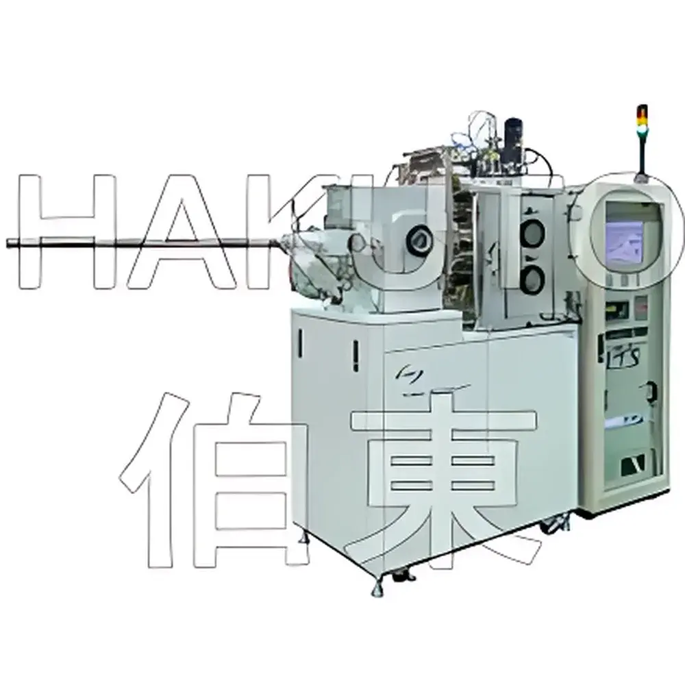
Syskey Co-Sputter Magnetron Sputtering Deposition System
| Brand | Syskey |
|---|---|
| Origin | Taiwan |
| Model | Co-Sputter |
| Instrument Type | Magnetron Sputtering Deposition System |
| Substrate Size | 12-inch (300 mm) |
| Substrate Temperature Range | Up to 1000 °C |
| Film Thickness Uniformity | ±3% |
| Base Pressure | 1×10⁻⁸ Torr |
| Sputter Sources | Up to 8 magnetron cathodes |
| Power Options | DC, Pulsed DC, RF |
| Gas Lines | Up to 4 mass flow controlled lines |
| Optional KRI Ion Source | Yes |
| Load-Lock Configuration | Single- or multi-wafer compatible |
| Vacuum Sealing | All-CF flanged, bakeable |
| Process Monitoring | Full-range vacuum gauges + Baratron capacitance manometer |
| Compliance | Designed for GLP/GMP-aligned thin-film R&D environments |
Overview
The Syskey Co-Sputter Magnetron Sputtering Deposition System is an advanced physical vapor deposition (PVD) platform engineered for high-precision, multi-target co-sputtering of complex thin films in semiconductor research, nanotechnology development, and functional materials synthesis. Based on the fundamental principles of magnetron sputtering—where plasma-generated argon ions bombard solid targets under magnetic confinement to eject atoms that subsequently condense onto heated or biased substrates—the system enables simultaneous, independent control of up to eight magnetron sources. This architecture supports both sequential layering and true co-deposition, making it ideal for fabricating multicomponent oxides (e.g., SiO₂, Al₂O₃), nitrides (e.g., Si₃N₄), metallic alloys (e.g., NbTiN, Pd), and emerging superconducting or catalytic thin films. The chamber achieves a base pressure of 1×10⁻⁸ Torr via all-CF flanged, bakeable ultra-high vacuum (UHV) construction—ensuring minimal residual gas contamination and superior film stoichiometry reproducibility.
Key Features
- Modular multi-source configuration: Supports up to eight independently powered magnetron cathodes (DC, pulsed DC, or RF), enabling precise stoichiometric tuning across conductive and insulating target materials.
- High-temperature substrate stage: Capable of uniform heating up to 1000 °C with active temperature feedback control; adjustable target-to-substrate distance ensures optimal ion flux distribution and minimizes shadowing effects.
- Integrated KRI ion source: Optional 100 eV Kaufman-type ion source provides in-situ substrate cleaning (via Ar⁺ sputter etching), surface activation prior to deposition, and ion-assisted densification during growth—critical for low-defect, high-adhesion films.
- Advanced process gas management: Four independently controlled MFCs deliver precise Ar, N₂, O₂, or reactive gas mixtures; load-lock compatibility enables rapid sample exchange without breaking main chamber vacuum.
- RF/DC bias capability: Independent substrate biasing (up to 300 W RF) allows controlled ion energy delivery for interface engineering, stress modulation, and enhanced nucleation density.
- Full UHV infrastructure: Cryo-pumped or turbo-molecular pumped chamber with all-metal CF seals, bakeable to 150 °C; equipped with full-range Pirani/cold cathode gauges and calibrated Baratron capacitance manometers for pressure stability monitoring.
Sample Compatibility & Compliance
The Co-Sputter system accommodates substrates up to 12-inch (300 mm) diameter wafers, with customizable chuck designs supporting flat, patterned, or fragile samples (e.g., TEM grids, flexible polymer foils). Its modular load-lock options—including single-wafer and cassette-based multi-wafer configurations—reduce pump-down time by >70% compared to batch loading, improving throughput in iterative R&D workflows. All hardware and software interfaces comply with international standards relevant to thin-film instrumentation: vacuum components conform to ISO 2861 and ASTM F2627; electrical safety meets IEC 61000-6-2/6-4; and optional audit trails, user-level access controls, and electronic signature support align with FDA 21 CFR Part 11 requirements for regulated GMP/GLP environments.
Software & Data Management
Operation is managed through a deterministic real-time control platform with synchronized logging of all process parameters—including power delivery per cathode, gas flows, chamber pressure, substrate temperature, bias voltage, and shutter actuation timing—at sub-second resolution. Raw data exports to CSV or HDF5 formats are fully timestamped and metadata-tagged (user ID, recipe name, run ID). Optional integration with LabVIEW™ or Python-based APIs enables automated recipe sequencing, closed-loop thickness control (when paired with in-situ quartz crystal microbalance or optical monitor), and remote diagnostics. All system logs retain immutable records for traceability—essential for method validation and regulatory submissions.
Applications
- Semiconductor device fabrication: High-k dielectrics (HfO₂, Al₂O₃), barrier layers (Ta/TaN), and metallization stacks (Cu/TiN).
- Nanomaterial synthesis: Compositionally graded transition metal nitrides, ferroelectric perovskites (e.g., BaTiO₃), and topological insulator heterostructures (Bi₂Se₃/Sb₂Te₃).
- Photovoltaics & optoelectronics: Transparent conducting oxides (ITO, AZO), anti-reflective coatings, and tandem cell interlayers.
- Quantum materials research: Epitaxial superconducting thin films (NbN, NbTiN), spintronic Heusler alloys, and 2D material heterointerfaces.
- Surface science & catalysis: Model catalyst thin films (Pt, Pd, NiO) with controlled grain size, oxidation state, and interfacial strain.
FAQ
What vacuum level is achievable, and how is it maintained?
Base pressure reaches ≤1×10⁻⁸ Torr using cryogenic or turbomolecular pumping combined with all-metal CF sealing and in-chamber baking capability. Continuous pressure monitoring is performed via redundant vacuum gauges including a calibrated Baratron for process-critical pressure stability.
Can the system deposit insulating films such as Al₂O₃ or SiO₂?
Yes—RF and pulsed DC power supplies enable stable sputtering from non-conductive ceramic targets. Reactive sputtering modes (e.g., O₂ + Ar for oxides) are fully supported with closed-loop gas ratio control.
Is in-situ film thickness monitoring supported?
The system includes standard flange ports for integrating quartz crystal microbalances (QCM) or optical emission spectroscopy (OES); optional ellipsometry or laser reflectometry interfaces are available upon request.
How is cross-contamination between targets prevented during co-sputtering?
Each magnetron cathode is fitted with individually actuated mechanical shutters; additional shadow masks and differential pumping zones minimize inter-target atom migration. Process recipes enforce strict shutter sequencing logic before and after each deposition step.
What level of technical support and documentation is provided?
Syskey delivers comprehensive installation qualification (IQ), operational qualification (OQ), and preventive maintenance protocols. Full schematics, safety manuals, and SOP templates compliant with ISO/IEC 17025 are included with delivery.


