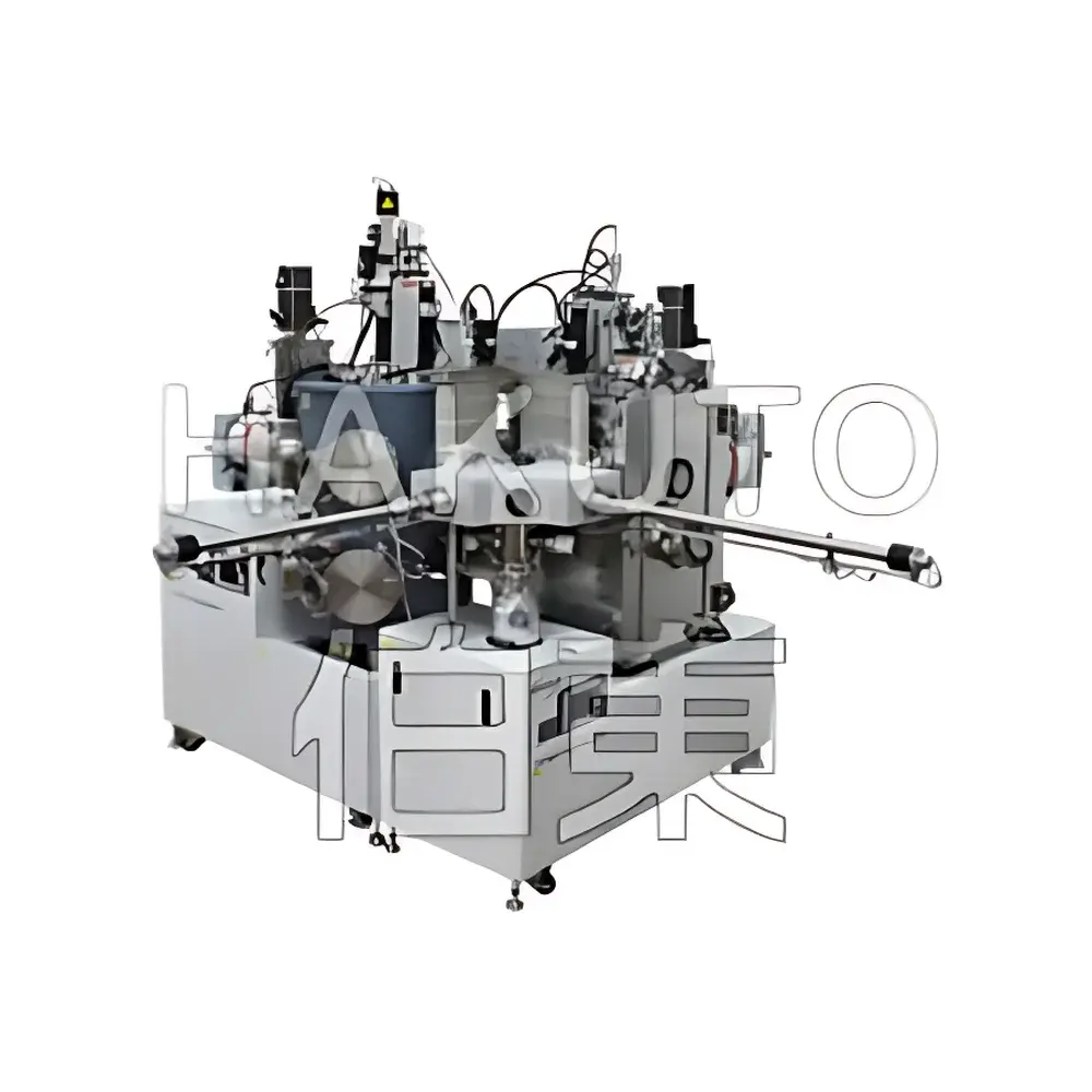
SYSKEY UHV E-beam Evaporation System for Thin Film Deposition
| Brand | SYSKEY |
|---|---|
| Origin | Taiwan |
| Manufacturer Type | Authorized Distributor |
| Instrument Type | Electron Beam Evaporator |
| Substrate Diameter | Up to 8 inches (203 mm) |
| Substrate Temperature Range | –70 °C (LN₂ cooling) to +800 °C |
| Thickness Uniformity | ±3% |
| Base Pressure | ≤5×10⁻¹⁰ Torr |
| E-beam Source Configuration | 4–6 crucibles (7–25 cm³ each) |
| Vacuum Sealing | All-metal CF flanges with bakeable elastomer O-rings |
| Pumping System | Cryopump (standard), optional turbomolecular pump |
| Process Monitoring | Bayard-Alpert gauge + quartz crystal microbalance (QCM) |
| Control Mode | Sequential or co-evaporation |
| Compliance | Designed for GLP/GMP-aligned thin-film R&D environments |
Overview
The SYSKEY UHV E-beam Evaporation System is a high-precision physical vapor deposition (PVD) platform engineered for reproducible, contamination-controlled thin-film growth under ultra-high vacuum (UHV) conditions. Operating at base pressures down to 5×10⁻¹⁰ Torr, the system eliminates residual gas-phase scattering and surface adsorption—critical for atomic-layer-sensitive applications in semiconductor device fabrication, optoelectronic research, and advanced functional material synthesis. Unlike thermal evaporation, electron beam evaporation delivers localized energy densities exceeding 3000 °C via focused electron bombardment, enabling uniform vaporization of refractory metals (e.g., W, Mo, Ta, Pt), oxides (e.g., ITO, TiO₂), and ceramic compounds that cannot be volatilized by resistive heating. The system integrates a rotationally symmetric substrate stage with active temperature control (–70 °C to +800 °C), water-cooled ceramic-bearing rotation mechanism, and bakeable all-metal vacuum architecture compliant with ISO-UHV standards (ISO 10110-9, ISO 20482).
Key Features
- UHV-compatible chamber with full CF-flange interconnects and bakeable sealing (up to 150 °C), ensuring long-term vacuum integrity and low outgassing rates.
- Modular e-beam source assembly supporting 4–6 independently controllable crucibles (7–25 cm³ volume), each equipped with water-cooled shielding to suppress thermal radiation cross-talk and minimize inter-material contamination.
- Motorized, center-aligned substrate rotation stage with precision ceramic bearings and integrated water-jacketed housing—designed for >10,000-hour continuous operation without drift or thermal deformation.
- Dual-mode substrate thermal management: liquid nitrogen cooling (–70 °C) for cryogenic film nucleation and resistive heating (up to 800 °C) with closed-loop PID control and thermocouple feedback.
- Real-time deposition rate monitoring via dual-channel quartz crystal microbalance (QCM), synchronized with e-beam power modulation for sub-nanometer thickness control.
- Programmable process logic supporting sequential layer deposition, simultaneous co-evaporation, and timed shutter sequencing—all traceable via timestamped log files.
Sample Compatibility & Compliance
The system accommodates substrates up to 8 inches (203 mm) in diameter—including Si, GaAs, sapphire, fused silica, and flexible metal foils—with flatness tolerance ≤±5 µm over full wafer area. Chamber geometry and source-to-substrate distance are configurable to optimize shadowing effects and step coverage for complex topographies. All wetted materials comply with ASTM F519 and SEMI F21 standards for semiconductor-grade vacuum compatibility. The vacuum architecture meets ISO 10110-9 requirements for UHV optical coating systems, while process logging and user access controls support alignment with FDA 21 CFR Part 11 and EU Annex 11 data integrity expectations for regulated R&D environments. Optional integration with load-lock modules, robotic transfer arms, and inert-atmosphere gloveboxes enables cluster-tool configurations for multi-step fabrication workflows.
Software & Data Management
Control is executed via a deterministic real-time operating system (RTOS) with deterministic I/O latency (<10 ms). The GUI provides intuitive layer-by-layer recipe definition, including e-beam current ramp profiles, shutter open/close timing, substrate rotation speed, and QCM-derived rate setpoints. All operational parameters—including vacuum status, thermocouple readings, e-beam emission current, and deposition thickness—are logged with millisecond resolution and exported in CSV/SQLite format. Audit trails record user login events, parameter modifications, and emergency stop triggers—fully compliant with GLP audit requirements. Optional OPC UA interface enables integration into factory-level MES or LIMS platforms for centralized data governance.
Applications
This system is routinely deployed in academic and industrial laboratories for: high-efficiency photovoltaic absorber layers (CIGS, perovskite precursors); low-loss dielectric stacks in VCSEL and DBR laser cavities; diffusion-barrier metallization (TiN, TaN) for advanced CMOS nodes; superconducting thin films (Nb, NbN, MgB₂); and epitaxial oxide heterostructures (LaAlO₃/SrTiO₃) requiring atomically clean interfaces. Its ability to evaporate high-melting-point materials without crucible reaction makes it indispensable for fabricating corrosion-resistant coatings, MEMS packaging layers, and quantum device electrodes where stoichiometric fidelity and interfacial purity are non-negotiable.
FAQ
What vacuum level is achievable with standard configuration?
Standard configuration achieves ≤5×10⁻¹⁰ Torr using a cryopump; optional turbomolecular pump + ion getter combination extends stability below 1×10⁻¹⁰ Torr for extended runs.
Can the system deposit multilayer structures with sub-nanometer interlayer control?
Yes—programmable shutter sequencing, QCM feedback, and <100 ms valve response time enable layer thickness control within ±0.3 nm for films <5 nm thick.
Is the chamber compatible with in-situ characterization tools?
Yes—multiple CF-63 and CF-100 ports support integration of RHEED, XPS, or ellipsometry viewports without compromising UHV integrity.
Does the system support automated recipe transfer between instruments?
Yes—recipe files are XML-based and interoperable across SYSKEY’s PVD platform family, facilitating process migration from R&D to pilot-line scale.
What maintenance intervals are recommended for e-beam source components?
Crucible liners require replacement after ~200 h of cumulative high-power operation; electron gun filaments are rated for ≥500 h at nominal current, with automated filament life tracking embedded in the control software.


