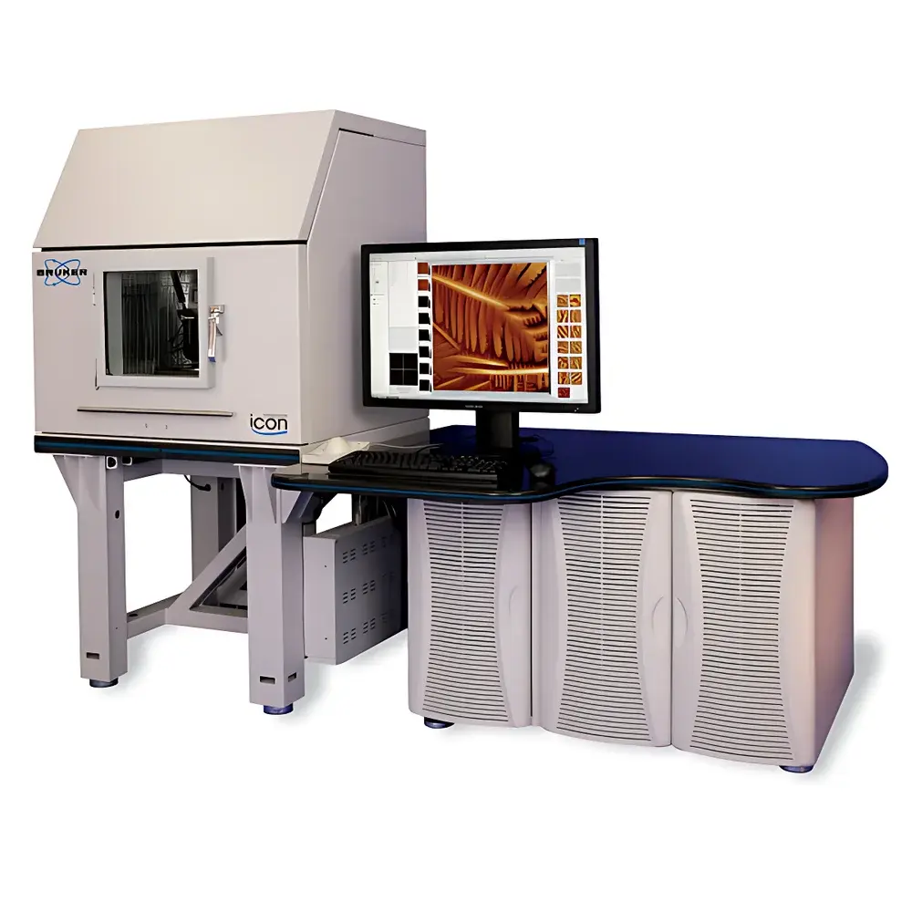
Bruker Dimension Icon Scanning Probe Microscope
| Brand | Bruker |
|---|---|
| Origin | USA |
| Model | Dimension Icon |
| Instrument Type | Atomic Force Microscope (AFM) |
| Vertical Noise Floor (Z-sensor, closed-loop) | <35 pm RMS |
| Typical Imaging Bandwidth | 625 Hz |
| Sample Stage | 210 mm vacuum chuck (Ø210 mm × 15 mm thick) |
| Stage Travel Range (X-Y visual field) | 180 mm × 180 mm |
| X-Y Scan Range (typical) | 90 µm × 90 µm |
| Z Scan Range (typical) | 10 µm |
| X-Y Positioning Noise (closed-loop) | <0.15 nm RMS (625 Hz) |
| Z Sensor Noise (closed-loop) | <35 pm RMS (625 Hz) |
| Overall Linearity Error (X-Y-Z) | 0.5% (typical) |
| Optical System | 5 MP digital camera, 180–1465 µm field of view, digital zoom & auto-focus |
| Controller | NanoScope V |
| Integrated Vibration Isolation | Monolithic pneumatic isolation table |
| Acoustic Enclosure | Rated for continuous ambient noise up to 85 dBC |
Overview
The Bruker Dimension Icon Scanning Probe Microscope is a high-performance, closed-loop atomic force microscope engineered for nanoscale metrology and quantitative surface characterization in research and industrial R&D environments. Built upon Bruker’s globally deployed Dimension platform, the Icon integrates decades of AFM innovation—including proprietary tip-scanning architecture, thermally compensated piezoelectric positioning sensors, and robust mechanical design—to deliver sub-ångström vertical resolution and ångström-level lateral stability under real-world lab conditions. Its measurement principle relies on optical beam deflection detection of cantilever bending, combined with real-time feedback control via low-noise, high-bandwidth closed-loop XYZ scanners. This architecture enables reliable topographic imaging, nanomechanical property mapping (e.g., modulus, adhesion, dissipation), and advanced dynamic modes—including HarmoniX multimodal nanomechanical spectroscopy—across diverse material classes including polymers, semiconductors, 2D materials, battery electrodes, and thin-film coatings.
Key Features
- Patented low-noise, thermally compensated XYZ closed-loop scanner delivering <0.15 nm RMS X-Y positioning noise and <35 pm RMS Z-sensor noise at 625 Hz bandwidth—enabling stable high-resolution imaging even on large-area samples.
- 90 µm × 90 µm typical scan range with 10 µm Z-range, optimized for both localized nanoscale analysis and extended-area survey mapping.
- 210 mm vacuum chuck stage (Ø210 mm × 15 mm max thickness) supporting wafers, substrates, and irregular specimens; motorized X-Y stage provides 180 mm × 180 mm visible field with ±3 µm bidirectional repeatability.
- Integrated 5-megapixel digital optical microscope with 180–1465 µm field-of-view, motorized focus, and digital zoom—enabling rapid sample navigation and precise probe alignment without manual repositioning.
- NanoScope V controller with FPGA-based real-time processing, supporting >100 standard and advanced AFM modes—including PeakForce Tapping®, ScanAsyst®, and HarmoniX—without hardware upgrades.
- Monolithic pneumatic vibration isolation table and acoustic enclosure certified for operation in ambient lab noise up to 85 dBC, eliminating need for dedicated cleanroom or basement installation.
Sample Compatibility & Compliance
The Dimension Icon accommodates a broad spectrum of sample geometries and material systems without requiring specialized mounting fixtures. Standard compatibility includes silicon wafers (up to 200 mm), TEM grids, polished metal coupons, polymer films, biological substrates (e.g., mica, HOPG, glass slides), and flexible electronics. The fully open sample chamber permits integration of environmental accessories—such as liquid cells, temperature-controlled stages (–30 °C to +250 °C), and electrical biasing modules—for in situ and operando measurements. From a regulatory standpoint, the system supports GLP/GMP-compliant workflows through NanoScope software’s audit trail functionality, electronic signature support, and user-access controls aligned with FDA 21 CFR Part 11 requirements. Data files adhere to standardized formats (e.g., Gwyddion-compatible .spm, HDF5 export) and are traceable to instrument configuration, calibration history, and operator metadata.
Software & Data Management
NanoScope Analysis software (v10.x and later) provides a modular, workflow-driven interface designed to reduce learning curves for new users while preserving full parameter control for experts. Preconfigured experiment templates—such as “Polymer Phase Imaging,” “Semiconductor Roughness QC,” or “Battery SEI Thickness Mapping”—encode best-practice settings for common applications. All raw data—including time-resolved force curves, spectral maps, and multi-channel images—are stored in hierarchical, self-documenting HDF5 containers. Batch processing tools enable automated flattening, filtering, roughness calculation (per ISO 25178), and statistical reporting across hundreds of datasets. Export options include CSV, TIFF, and MATLAB-compatible formats, facilitating integration with third-party analysis platforms such as Python-based SciPy stacks or MATLAB Image Processing Toolbox.
Applications
The Dimension Icon serves as a core characterization tool in academic, government, and industrial laboratories focused on nanomaterials development and process optimization. Key use cases include: quantitative surface roughness and step-height metrology for semiconductor photomasks (per SEMI/ASTM E2522); nanomechanical mapping of polymer blend phase separation; grain boundary analysis in perovskite solar cell layers; interfacial stiffness profiling across solid-electrolyte interphases (SEI) in Li-ion batteries; and nanoscale wear and adhesion quantification in tribological coatings. Its high-speed closed-loop scanning and HarmoniX mode also support statistically robust nanoindentation arrays over 100×100 µm areas—enabling correlation of local mechanical properties with microstructural features observed via SEM or XRD.
FAQ
What sample preparation is required for standard tapping-mode imaging?
Minimal preparation is needed: conductive samples (e.g., Si wafers) require only cleaning with solvents; insulating samples may benefit from light sputter-coating (e.g., 2 nm Cr/Au) if charge accumulation interferes with feedback stability.
Can the Dimension Icon operate in liquid environments?
Yes—via optional fluid cells compatible with electrochemical AFM (EC-AFM), biological buffer imaging, and corrosion studies. All fluid cell designs maintain full closed-loop performance and optical access.
Is remote operation supported for multi-user facilities?
Yes—NanoScope software supports secure remote desktop access and scheduled instrument queuing via Bruker’s LabConnect™ server module, enabling shared resource management across distributed teams.
How is calibration traceability maintained?
Bruker provides NIST-traceable calibration artifacts (gratings, step-height standards) and software-assisted calibration routines compliant with ISO/IEC 17025 guidelines for metrological validation.
Does the system support third-party probes and custom cantilevers?
Yes—the Icon uses industry-standard probe holders and accepts all commercial AFM probes (e.g., Bruker, Nanoworld, Olympus), including conductive, magnetic, and high-aspect-ratio variants.


