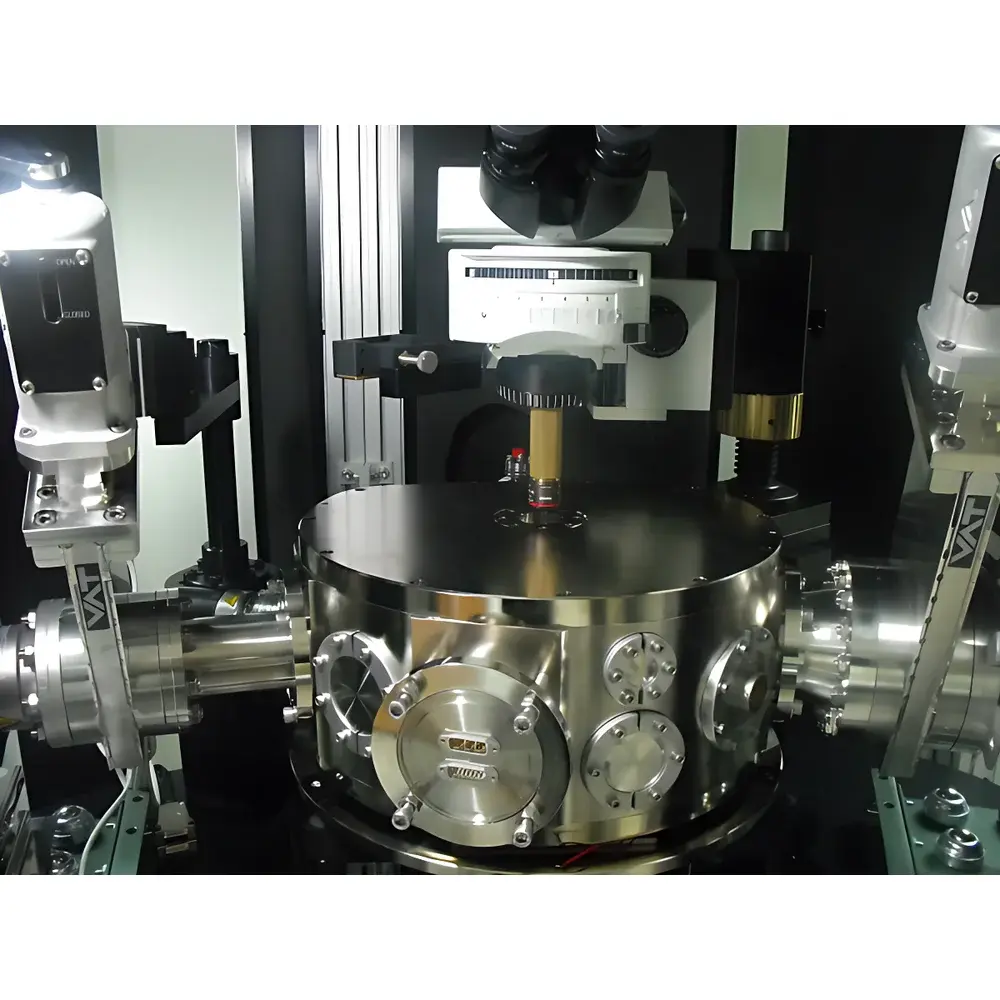
Nanonics CryoView4000 Low-Temperature Ultra-High-Vacuum Near-Field Optical Scanning Probe Microscope
| Brand | Nanonics |
|---|---|
| Origin | Israel |
| Model | CryoView4000 |
| Z-positioning noise | <0.2 nm |
| Sample diameter | <100 mm |
| Sample thickness | <30 mm |
| Sample stage travel range | 80 µm × 80 µm × 70 µm |
Overview
The Nanonics CryoView4000 is a fully integrated, ultra-high-vacuum (UHV) compatible, cryogenic scanning probe microscope engineered for concurrent nanoscale structural imaging, multi-probe electrical/thermal/optical property mapping, and in situ nanofabrication. Unlike conventional AFM platforms reliant on optical beam deflection feedback—which introduces spurious electrostatic charging, thermal drift, and optical interference—the CryoView4000 employs patented tuning-fork-based force detection with sub-piconewton sensitivity, enabling true non-perturbative operation under UHV and cryogenic conditions (down to 4 K). Its core architecture supports simultaneous multi-probe coordination (up to four independently controlled probes), including conductive AFM, scanning tunneling microscopy (STM), nano-manipulation probes, and near-field optical (NSOM/SNOM) apertured or plasmonic tips. This platform uniquely unifies high-resolution topographic imaging, quantitative nanoelectrical transport measurement (e.g., I–V spectroscopy, Kelvin probe force microscopy), localized photoluminescence excitation, tip-enhanced Raman spectroscopy (TERS), and real-time nanoscale oxidation/reduction processing—all within a single, optically accessible vacuum chamber.
Key Features
- Ultra-low-noise Z-positioning (<0.2 nm RMS) enabled by monolithic quartz tuning-fork transducers and low-thermal-drift piezoelectric actuators
- Full optical access along vertical and inverted optical axes—compatible with research-grade upright and inverted microscopes for real-time probe navigation and correlative optical-SPM imaging
- Integrated cryogenic cooling system (4–350 K) with active temperature stabilization and programmable ramping profiles
- UHV-compatible sample chamber (base pressure <1×10⁻⁹ mbar) with bake-out capability and differential pumping for optical path integrity
- Modular multi-probe tower supporting simultaneous use of AFM, STM, nano-manipulator, and NSOM/TERS probes—each with independent XYZ positioning and electrical biasing
- Patented NanoToolKit™ probe design enabling physical probe-to-probe contact imaging and inter-probe conductivity mapping at sub-nanometer separation
- No laser-based feedback loop—eliminates photo-induced charge trapping, background photocurrents, and optical crosstalk during electrical or optical measurements
Sample Compatibility & Compliance
The CryoView4000 accommodates planar solid-state samples up to 100 mm in diameter and 30 mm in thickness, including exfoliated 2D materials (graphene, TMDCs), epitaxial thin films, superconducting oxides, topological insulators, and hybrid perovskite heterostructures. All mechanical and electrical interfaces conform to ISO 9001-certified manufacturing standards. The system’s vacuum architecture complies with ASTM E577 (Standard Practice for Vacuum System Integrity Testing) and supports GLP-compliant operation through hardware-enforced audit trails, timestamped parameter logging, and user-accessible raw data export (HDF5, ASCII). Optional integration with FDA 21 CFR Part 11–compliant software modules enables regulated environments requiring electronic signatures and data integrity verification.
Software & Data Management
The proprietary MultiView™ acquisition and analysis suite provides synchronized control of all probe modalities, environmental parameters (temperature, pressure, gas dosing), and external optical sources (tunable lasers, CW/pulsed diodes, spectrometers). Real-time data streaming supports simultaneous recording of topography, current maps, surface potential, photon counts, and Raman spectra at pixel rates exceeding 100 Hz. All datasets are stored in self-describing HDF5 containers with embedded metadata (probe type, calibration constants, environmental state, timestamp). Batch processing pipelines support automated baseline correction, spectral deconvolution (Voigt fitting), conductance quantization analysis, and spatial correlation of optical and electronic signals. Export modules comply with FAIR data principles (Findable, Accessible, Interoperable, Reusable) and interface natively with Python (via PyNanonics SDK), MATLAB, and Igor Pro.
Applications
- Atomic-scale defect characterization in van der Waals heterostructures via correlated STM/AFM/TERS
- In situ observation of phase transitions (e.g., charge density waves, superconducting gap evolution) under variable temperature and bias
- Nanoscale photocarrier dynamics mapping using time-resolved NSOM with pulsed excitation
- Tip-induced local oxidation and chemical functionalization with simultaneous work-function monitoring
- Quantitative mapping of electron–phonon coupling strength via spatially resolved TERS on monolayer MoS₂
- Correlative cryo-SPM/optical microscopy of quantum dot arrays and plasmonic metasurfaces
- Electrochemical SPM studies of solid–electrolyte interphases (SEI) in battery materials under inert UHV conditions
FAQ
What vacuum level does the CryoView4000 achieve, and how is it maintained during optical experiments?
The base pressure is <1×10⁻⁹ mbar, achieved using a combination of turbomolecular pumping, ion gettering, and cryoshielding. Differential pumping isolates the optical path from the main chamber, preserving transmission efficiency for visible–NIR wavelengths.
Can the system perform simultaneous electrical transport and near-field optical spectroscopy?
Yes—dedicated low-noise current preamplifiers (1 fA resolution) and fiber-coupled spectrometers operate concurrently with NSOM illumination, with full electromagnetic shielding and grounding isolation.
Is probe-to-probe imaging limited to conductive probes?
No—NanoToolKit™ probes include both metallic and dielectric variants; mechanical contact imaging is achieved via tuning-fork frequency shift, independent of electrical conductivity.
How is thermal drift compensated during long-duration cryogenic scans?
Real-time drift correction uses a dual-reference interferometric position sensor integrated into the sample stage, updated at 1 kHz and applied as feed-forward compensation to all scan axes.
Does the system support gas-phase nanofabrication (e.g., H₂O, O₂, NH₃ dosing)?
Yes—integrated mass-flow-controlled gas inlets with UHV-compatible valves enable reactive nanofabrication under precisely defined partial pressures (10⁻⁸–10⁻⁴ mbar range).


