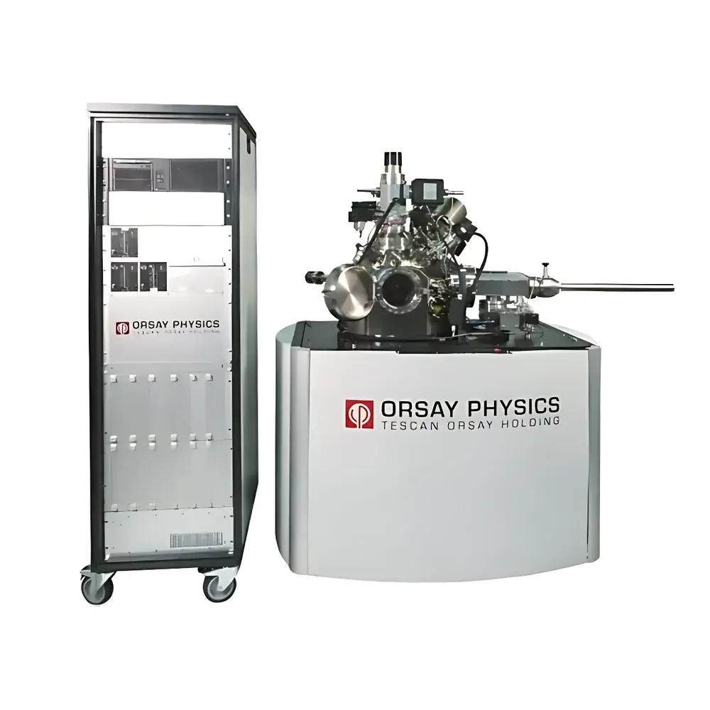
TESCAN NanoSpace Custom Ultra-High Vacuum Multi-Beam Electron Microscopy System
| Brand | TESCAN |
|---|---|
| Origin | Czech Republic |
| Manufacturer Type | Original Equipment Manufacturer (OEM) |
| Origin Category | Imported |
| Model | NanoSpace |
| Price Range | USD 1.9M – 3.2M |
| Main Chamber Base Pressure | 5 × 10⁻¹⁰ mbar |
| Bake-Out Temperature | Up to 120 °C |
| Sample Transfer Time (Atmosphere → UHV Main Chamber) | ≤30 min |
| Stage X/Y Travel Range | 100 mm ± 50 nm |
| BrightBeam e-Optics Resolution | <1.6 nm @ 12 mm WD, 0.5–30 keV, beam current: few pA to >350 nA |
| e-CLIPSE+ e-Optics Resolution | 5 nm @ 1 pA, 0.5–30 keV, beam current: 1 pA–2.5 µA @ 30 keV, FOV @ 10 keV: 1250 × 1250 µm (±10%) |
| DeepFIB Ga⁺ Source Resolution | 2.5 nm @ 1 pA, 250 V–30 keV, max ion current: 125 nA |
| PFIB Gas Field Ion Source (Xe⁺/O₂⁺/Ar⁺/He⁺/N⁺) | 25 nm @ 1 pA @ 3 keV, beam current up to 3.5 µA, FOV @ 10 keV: 1250 × 1250 µm (±10%), Si milling rate: 800 µm³/s |
| Veloce LMAIS (AuGe/AuSi/Bi) | 5 nm @ 1 pA, mass range: 14 (Si⁺) to 613 (AuSi⁺), 1–30 keV, max current: 50 nA |
| iVeloce Wien-filtered Gas Ion Source (Xe⁺/O₂⁺/Ar⁺/He⁺/N⁺) | 3–30 keV, max current: 1 µA, FOV @ 10 keV: 1250 × 1250 µm (±10%) |
Overview
The TESCAN NanoSpace Custom Ultra-High Vacuum Multi-Beam Electron Microscopy System is an engineered platform for in situ nanoscale characterization and manipulation under rigorously controlled ultra-high vacuum (UHV) conditions. Designed around a modular, multi-column architecture, the NanoSpace integrates one or more high-performance electron optical columns with complementary focused ion beam (FIB) columns—including gallium liquid metal ion sources (LMIS), plasma-based gas field ion sources (GFIS), Wien-filtered liquid metal alloy ion sources (LMAIS), and Wien-filtered multi-gas ion sources—within a single UHV main chamber. Its base pressure of 5 × 10⁻¹⁰ mbar—achievable via full-system bake-out to 120 °C—ensures surface-sensitive analytical integrity by suppressing hydrocarbon contamination, adsorption-induced surface reconstruction, and residual gas-induced beam-induced damage. This performance exceeds standard high-vacuum SEM/FIB systems by four to five orders of magnitude, enabling applications requiring atomic-scale surface cleanliness: epitaxial interface analysis, native oxide characterization, catalytic surface reaction studies, and correlative secondary ion mass spectrometry (SIMS) mapping.
Key Features
- UHV-compliant mechanical and thermal design: All internal components—including stage, detectors, apertures, and column interfaces—are constructed from low-outgassing materials (e.g., oxygen-free copper, stainless steel 316L, ceramic insulators) and qualified for sustained bake-out at 120 °C.
- Modular multi-beam configuration: Users select from interchangeable FIB columns—DeepFIB (Ga⁺), PFIB (Xe⁺/O₂⁺/Ar⁺/He⁺/N⁺), Veloce (AuGe/AuSi/Bi LMAIS), or iVeloce (Wien-filtered multi-gas)—without compromising UHV integrity or alignment stability.
- Correlative SIMS-ready geometry: The multi-column layout enables precise spatial registration between high-resolution SEM imaging (using YAP-scintillator-based SE detection) and time-of-flight or magnetic sector SIMS analysis, supporting quantitative depth profiling and isotopic mapping.
- Six-axis UHV-compatible sample stage: Supports samples up to 100 mm × 100 mm with sub-50 nm positional repeatability; integrated heating/cooling options available for in situ thermal experiments.
- UHV transfer interlock chamber: Equipped with differential pumping stages and gate valves compliant with ISO-KF 100 and CF 150 standards, enabling direct integration with external UHV systems such as molecular beam epitaxy (MBE) clusters, atom probe tomography (APT) instruments, or synchrotron beamlines.
- Fully automated vacuum sequencing: Integrated PLC-controlled turbomolecular and ion pump arrays, backed by real-time partial pressure monitoring (RGA), ensure reproducible pump-down cycles (<30 min from atmosphere to operational UHV) and fail-safe interlocks per ISO 27416-1.
Sample Compatibility & Compliance
The NanoSpace accommodates conductive and non-conductive specimens—including semiconductors, oxides, 2D materials, and catalytic nanoparticles—without mandatory sputter coating, owing to its low-noise, high-efficiency YAP scintillator detector and beam-induced charge compensation capabilities. All UHV subsystems conform to ISO 14644-1 Class 4 cleanroom requirements during assembly and are certified to EN 61000-6-4 (EMC emission) and EN 61000-6-2 (immunity). The system supports GLP-compliant operation through audit-trail-enabled software logging (per FDA 21 CFR Part 11 Annex 11), including timestamped vacuum logs, beam parameter history, and user access records. Optional UHV-compatible gas injection systems (GIS) meet ASTM E2752-20 specifications for localized deposition (e.g., Pt/C, W, Ir) and selective etching (e.g., XeF₂, I₂).
Software & Data Management
Control and acquisition are managed entirely through Orsay Physics’ Pegasus software—a client-server application built on TCP/IP architecture with deterministic real-time beam control. Pegasus provides synchronized multi-beam scripting (e.g., sequential SEM imaging → FIB milling → SIMS rastering), automated drift correction via fiducial tracking, and vendor-neutral data export in HDF5 format compliant with the FAIR principles (Findable, Accessible, Interoperable, Reusable). Raw image and spectrum datasets include embedded metadata per the ISO/IEC 11179 standard, covering instrument configuration, vacuum status, beam parameters, and calibration certificates. Remote diagnostics and firmware updates are supported via TLS-encrypted channels, ensuring cybersecurity compliance with NIST SP 800-171.
Applications
- Atomic-layer-resolved cross-sectional analysis of heterostructures (e.g., GaN-on-Si, MoS₂/h-BN) without interfacial oxidation artifacts.
- In situ FIB-induced phase transformation studies under controlled thermal bias (e.g., crystallization of amorphous GeTe, strain relaxation in strained-SiGe).
- Quantitative SIMS isotopic imaging of dopant segregation at grain boundaries in polycrystalline PV materials.
- UHV-integrated MBE-NanoSpace workflows for real-time growth monitoring and defect engineering verification.
- Atom probe tomography specimen preparation with minimized surface damage and field evaporation artifacts.
- Correlative cathodoluminescence (CL) and SIMS mapping of quantum dot emission centers and associated impurity distributions.
FAQ
What vacuum level is required for SIMS coupling, and how does NanoSpace achieve it?
NanoSpace achieves a base pressure of 5 × 10⁻¹⁰ mbar via all-metal sealing, low-outgassing materials, and programmable 120 °C bake-out—meeting the stringent vacuum requirements for high-mass-resolution SIMS (typically <1 × 10⁻⁹ mbar).
Can the system operate with multiple ion sources simultaneously?
Yes—the modular column architecture and independent differential pumping allow concurrent operation of up to three beams (e.g., SEM + Ga⁺ FIB + Xe⁺ PFIB), with beam blanking and stigmation fully decoupled.
Is Pegasus software compatible with third-party automation frameworks?
Pegasus exposes RESTful APIs and Python bindings for integration with LabVIEW, MATLAB, or custom Python-based experiment orchestration platforms, supporting scheduled multi-step workflows.
What certifications apply to the UHV transfer interface?
The interlock chamber complies with ISO-KF 100/CF 150 flange standards and includes helium-leak-tested welds certified to ASME BPVC Section VIII, Division 1.
How is beam alignment maintained after bake-out cycles?
All optical columns feature in-situ electrostatic/magnetic alignment actuators calibrated against a reference grid; alignment drift is corrected automatically using Pegasus’ iterative centroid-tracking algorithm.


