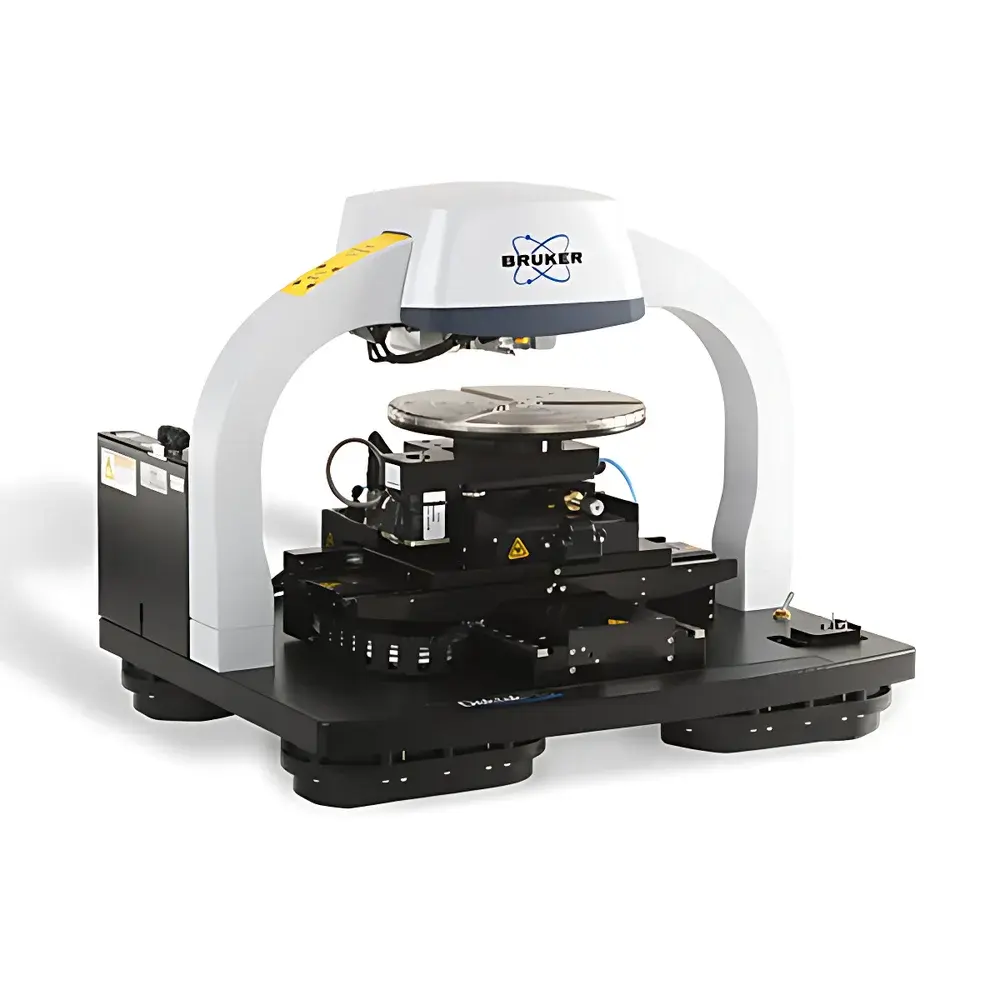
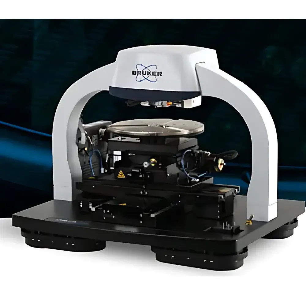
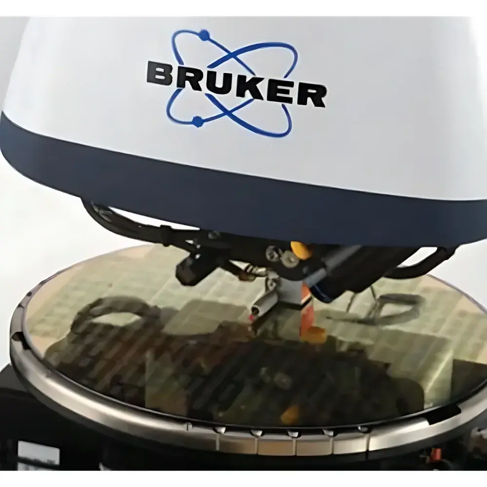
Bruker Dektak Pro Stylus Profilometer
| Brand | Bruker |
|---|---|
| Origin | Germany |
| Model | Dektak Pro |
| Measurement Repeatability | 4 Å |
| Accuracy | ±1% |
| Probe Tip Radius | 50 nm – 25 µm |
| Normal Force Range | 0.03–15 mg |
| Scan Length | 55 mm |
| Step Height Repeatability | 4 Å |
| Vertical Resolution | 1 Å |
| Maximum Sample Size | 200 mm |
Overview
The Bruker Dektak Pro is a high-performance stylus profilometer engineered for precision surface topography characterization in research and industrial metrology environments. It operates on the contact-based mechanical scanning principle: a diamond-tipped probe traverses the sample surface under controlled normal force, converting vertical displacement into high-fidelity analog voltage signals via a low-inertia sensor (LIS 3). This analog signal is digitized with 24-bit resolution and processed to generate quantitative 2D and 3D surface profiles. Designed as the 11th-generation evolution of the Dektak platform, the Dektak Pro delivers sub-angstrom vertical resolution (1 Å) and exceptional measurement repeatability (≤4 Å on 1 µm step standards), making it suitable for critical applications where nanoscale dimensional fidelity is non-negotiable — including thin-film stress evaluation, wafer bow mapping, and microfabricated feature metrology.
Key Features
- Single-arch mechanical architecture minimizing sensitivity to environmental vibration and acoustic noise, enabling stable operation in standard lab environments without active isolation.
- Direct-drive scanning stage delivering high-speed, high-resolution profiling over 55 mm travel length with negligible mechanical hysteresis or backlash.
- Low-inertia sensor (LIS 3) enabling rapid dynamic response to abrupt surface topography changes — essential for accurate measurement of steep sidewalls, trench edges, and MEMS structures.
- Self-aligning probe holder allowing full probe replacement in under 60 seconds without realignment or system recalibration.
- Wide-force range capability: 0.03–15 mg (with N-Lite+ mode extending down to ultra-low-force regime), supporting delicate soft films and robust hard coatings alike.
- Integrated optical viewing system with minimized chromatic and spherical aberration, ensuring consistent focus across full field-of-view for precise feature targeting.
Sample Compatibility & Compliance
The Dektak Pro accommodates substrates up to 200 mm in diameter, including full-size wafers, glass panels, and polymer sheets. Its modular probe selection (tip radii from 50 nm to 25 µm) and programmable force control ensure compatibility with diverse material classes: silicon nitride membranes, photoresist patterns, biomedical hydrogels, metallic thin films, and oxide dielectrics. The system supports traceable calibration per ISO/IEC 17025 requirements and enables audit-ready data acquisition compliant with FDA 21 CFR Part 11 when deployed with Vision64 software configured for electronic signatures and secure user access controls. All measurement routines adhere to ASTM E1087 (standard test method for measuring step height using stylus instruments) and ISO 25178-2 (areal surface texture parameters).
Software & Data Management
Vision64® is a native 64-bit software platform optimized for multi-core processing and large dataset handling. It provides intuitive workflow-driven measurement setup, automated recipe execution, and GLP/GMP-compliant data archiving. Key capabilities include real-time auto-leveling, adaptive noise filtering, intelligent edge detection, and fully customizable report generation. All raw scan data are stored in Bruker’s proprietary .pro format (HDF5-based), preserving metadata such as probe ID, force setting, scan speed, calibration timestamp, and operator credentials. Audit trails record every parameter change, file export, and user login event — supporting regulatory inspections and internal QA/QC documentation.
Applications
- Microelectronics: Monitoring etch depth uniformity, quantifying gate stack thickness, evaluating trench profile asymmetry, and characterizing interconnect step coverage.
- Thin Films & Coatings: Measuring UV-curable lens coatings, decorative PVD layers on faucets, inkjet-printed conductive traces, and anti-reflective multilayer stacks.
- Life Sciences: Profiling microfluidic channel geometry, assessing collagen film thickness on biosensor substrates, and quantifying cell monolayer height variations post-stimulation.
- Materials Science: Calculating biaxial film stress via wafer curvature analysis (Stoney equation), mapping localized stress gradients in graded oxide films, and correlating roughness parameters (Sa, Sq, Sz) with adhesion performance.
FAQ
What is the minimum measurable step height with the Dektak Pro?
The system can resolve steps as low as 1 nm under optimal conditions; repeatability of ≤4 Å is guaranteed on certified 1 µm step standards.
Does the Dektak Pro support automated multi-site measurement?
Yes — Vision64 enables programmable XY stage navigation, pattern-based site selection, and batch execution of identical measurement protocols across multiple locations.
Can the Dektak Pro measure surface roughness per ISO 25178?
Yes — it calculates areal roughness parameters (Sa, Sq, Sz, Sk, Spk, Svk) directly from acquired 2D line scans and supports stitching for extended-area analysis.
Is thermal drift compensation built into the system?
Yes — advanced thermal management and low-drift analog electronics reduce temperature-induced baseline drift to <0.5 Å/°C over typical lab ambient fluctuations.
How does probe wear affect measurement accuracy?
Vision64 includes real-time probe condition monitoring and automatic tip radius verification routines; worn probes trigger configurable alerts prior to data degradation.