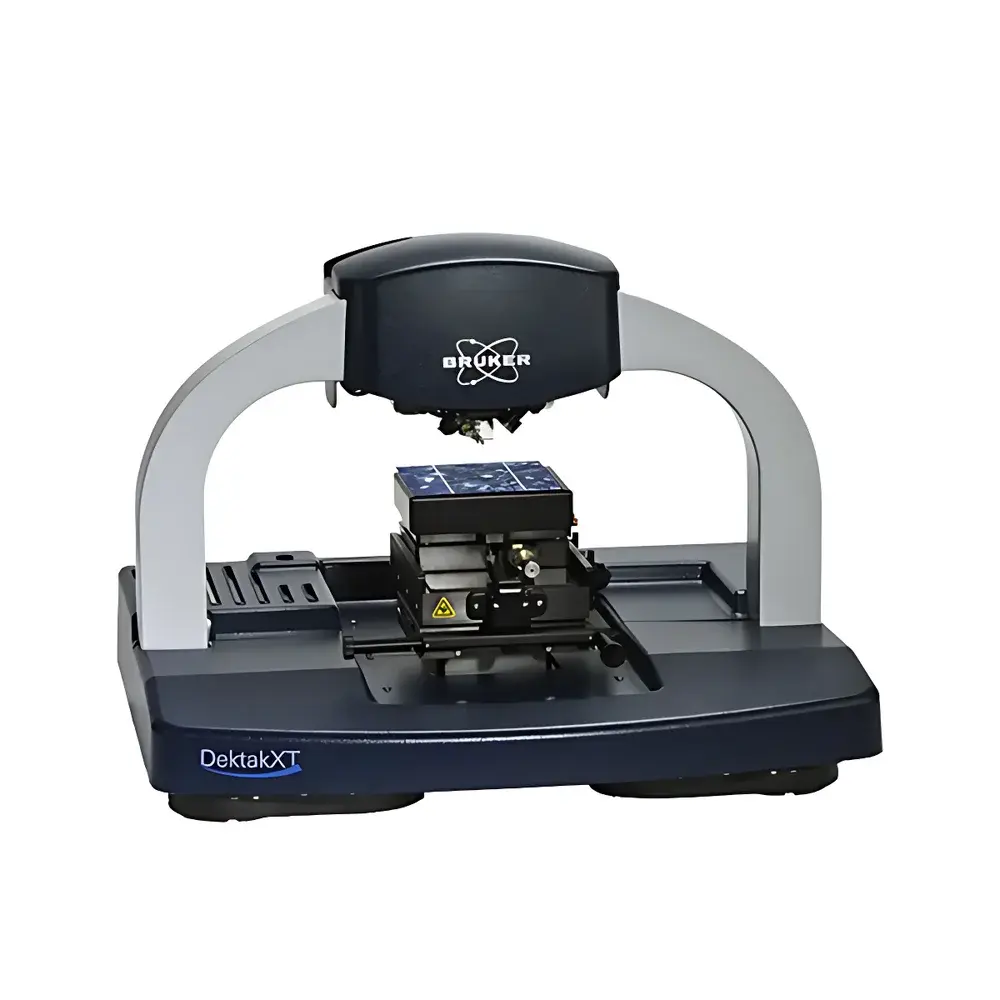
Bruker DEKTAK XT Stylus Profilometer
| Brand | Bruker |
|---|---|
| Origin | Germany |
| Model | DEKTAK XT |
| Measurement Principle | Contact Stylus Profilometry |
| Vertical Resolution | 1 Å |
| Step Height Repeatability | <4 Å |
| Vertical Measurement Range | Up to 1 mm |
| Probe Tip Radius | 50 nm – 25 µm |
| Normal Force | 15 µN (adjustable) |
| Scan Length | 55 mm (2-inch stage travel) |
| Maximum Sample Size | 50 mm diameter |
| Accuracy | ±1% of measured value |
| Horizontal Positioning Resolution | 10 nm |
| Data Acquisition Speed | 40% faster than previous generation |
Overview
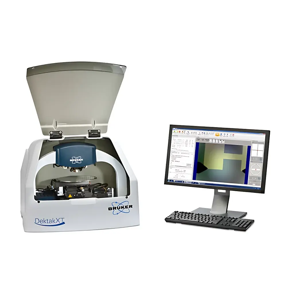
The Bruker DEKTAK XT Stylus Profilometer is an advanced contact-based surface metrology instrument engineered for high-precision, nanoscale step height and surface topography characterization. Operating on the principle of inductive stylus displacement sensing, the DEKTAK XT translates physical probe deflection—induced by surface elevation changes—into quantitative vertical profiles with sub-angstrom resolution. Its core architecture integrates a single-arch mechanical design, direct-drive scanning stage, and low-noise smart electronics to minimize environmental interference and ensure exceptional thermal and mechanical stability. Designed for both R&D laboratories and production QA/QC environments, the system delivers traceable, reproducible measurements compliant with ISO 25178 (Geometrical Product Specifications – Surface Texture) and ASTM E1316 (Standard Terminology for Nondestructive Examinations), supporting critical process control in semiconductor fabrication, thin-film deposition, MEMS development, and medical device manufacturing.
Key Features
- Single-arch structural architecture delivering superior rigidity and vibration immunity, enabling stable long-scan measurements under ambient lab conditions.
- Direct-drive sample stage with 55 mm travel range and 10 nm positioning resolution, reducing mechanical hysteresis and improving scan repeatability.
- Smart electronics platform featuring low-noise analog front-end and real-time digital signal processing, optimized for sub-10 nm step detection at forces as low as 15 µN.
- Auto-aligning probe cartridge system allowing rapid, repeatable stylus exchange without recalibration or alignment tools—reducing downtime and operator dependency.
- Modular probe library supporting tip radii from 50 nm to 25 µm, enabling application-specific optimization for soft polymer films, hard sputtered coatings, or high-aspect-ratio microstructures.
- Integrated NLite+ force control mode for ultra-low-force profiling of delicate photoresists, hydrogels, and biomaterials without surface deformation.
Sample Compatibility & Compliance
The DEKTAK XT accommodates wafers and substrates up to 50 mm in diameter, including silicon, glass, fused silica, metal foils, and flexible polymer sheets. Its open-stage configuration supports custom fixtures for non-standard geometries such as curved implants or segmented solar cells. All measurement data are timestamped, user-logged, and stored with full audit trail metadata—fully compatible with GLP/GMP workflows and FDA 21 CFR Part 11 requirements when deployed with Vision64 software’s electronic signature and role-based access controls. Calibration is traceable to NIST standards via Bruker-certified reference standards (e.g., SiO₂-on-Si step height standards), and system performance verification follows ISO 21243 (Stylus Instruments – Verification Procedures).
Software & Data Management
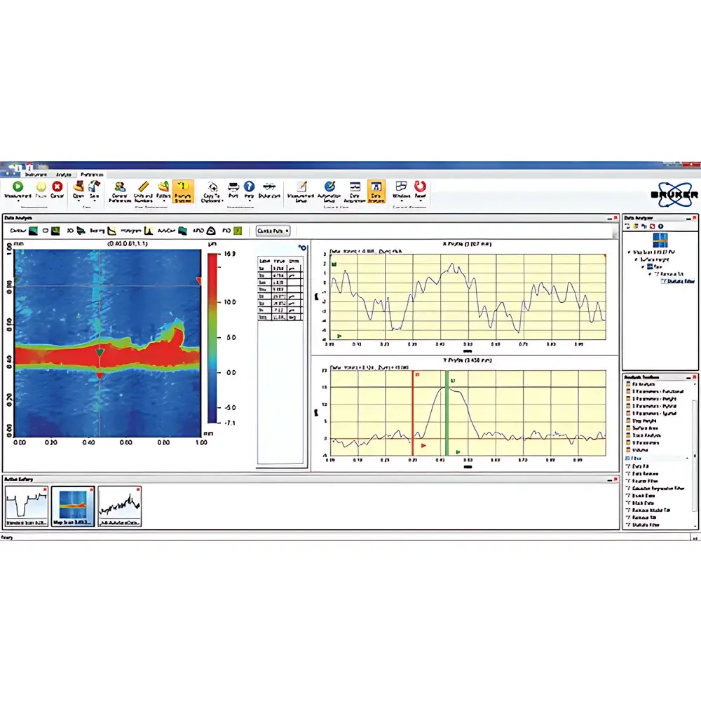
Vision64 is Bruker’s native 64-bit parallel processing software platform, enabling real-time acquisition, filtering, and analysis of large-area 3D topography datasets. It features multi-threaded algorithms for Gaussian, Spline, and Robust polynomial filtering; automated step height, roughness (Sa, Sq, Sz per ISO 25178-2), and film stress calculation; and customizable pass/fail templates aligned with internal quality specifications. Raw data are saved in Bruker’s proprietary .pro format (XML-based, human-readable metadata) and exportable to ASCII, CSV, or industry-standard formats (e.g., .stp, .xyz). Vision64 supports batch scripting, recipe-driven automation, and integration with factory MES systems via OPC UA or TCP/IP protocols—ensuring seamless data flow into statistical process control (SPC) dashboards.
Applications
- Semiconductor Process Monitoring: Quantifying etch/deposition uniformity across 200 mm wafers; measuring ITO thickness and stress on touch panel substrates; validating lithographic lift-off profiles.
- Thin-Film Stress Analysis: Extracting biaxial stress values from curvature-induced step height gradients using Stoney’s equation implementation within Vision64.
- Medical Device Surface Characterization: Assessing HA (hydroxyapatite) coating roughness on orthopedic implants per ISO 13779-2; verifying surface texture compliance prior to sterilization.
- Photovoltaic Metrology: Measuring silver gridline height, width, and continuity on mono-/polycrystalline Si solar cells to correlate morphology with series resistance and fill factor.
- MEMS & Microfluidics: Profiling SU-8 mold heights, PDMS replica fidelity, and channel depth uniformity with <4 Å repeatability over 1 mm vertical range.
FAQ
What is the minimum detectable step height on the DEKTAK XT?
The system achieves a step height repeatability of <4 Å (0.4 nm) under optimal conditions, making it suitable for atomic-layer-deposited film thickness verification.
Can the DEKTAK XT measure rough surfaces with high aspect ratios?
Yes—using probes with larger tip radii (up to 25 µm) and NLite+ force control, the instrument maintains fidelity on surfaces with slopes exceeding 70° and vertical ranges up to 1 mm.
Is Vision64 software compliant with regulatory data integrity requirements?
When configured with user authentication, electronic signatures, and audit trail logging enabled, Vision64 meets FDA 21 CFR Part 11 and EU Annex 11 expectations for regulated environments.
How does the DEKTAK XT handle thermal drift during extended scans?
The single-arch aluminum frame and thermally isolated probe carriage reduce coefficient-of-thermal-expansion mismatch, limiting vertical drift to <0.5 nm/°C over typical 2-hour measurement sessions.
Does Bruker provide certified calibration standards for routine verification?
Yes—NIST-traceable step height standards (e.g., 10 nm, 100 nm, 1 µm SiO₂-on-Si wafers) and roughness standards (Ra 0.05–5.0 µm) are available with full uncertainty budgets and calibration certificates.