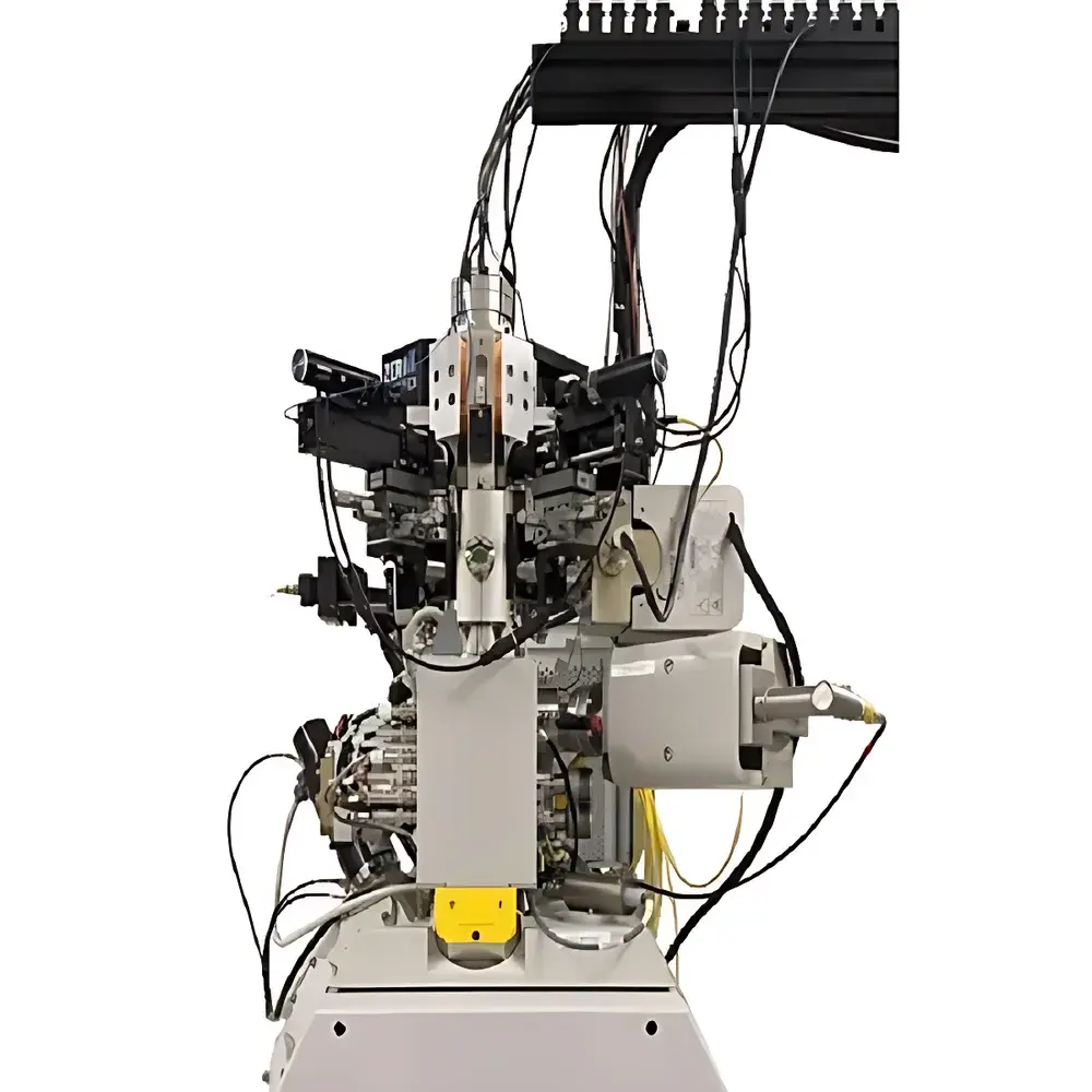
zeroK FIB:ZERO Cryogenic Cesium Ion Source Focused Ion Beam System
| Brand | zeroK |
|---|---|
| Origin | USA |
| Model | FIB:ZERO (Cs⁺ LoTIS) |
| Ion Source Type | Cryogenically Cooled Cesium Ion Source (LoTIS) |
| Resolution | ≤2 nm @ 10 keV |
| Beam Current Range | 1 pA – >10 nA |
| Acceleration Voltage | 2–18 kV |
| Secondary Ion Yield | Enhanced vs. Ga⁺/He⁺/Ne⁺ |
| SIMS Compatibility | Full dynamic SIMS integration |
| Compliance | ASTM E1558, ISO/IEC 17025-aligned operation, GLP/GMP-ready data audit trail |
Overview
The zeroK FIB:ZERO is a next-generation focused ion beam (FIB) system engineered for ultra-high spatial resolution nanofabrication, analytical imaging, and site-specific sample preparation—leveraging cryogenically cooled cesium ion source (Cs⁺ LoTIS) technology. Unlike conventional liquid metal ion sources (e.g., Ga⁺ LMIS) or noble gas ion sources (He⁺, Ne⁺), the FIB:ZERO employs laser-cooled atomic beam ionization—a Nobel-recognized methodology—to suppress thermal motion in the Cs⁺ ion beam. This results in reduced transverse energy spread (1 × 10⁸ A·sr⁻¹·cm⁻²), and sub-2 nm probe convergence at 10 keV. The system operates on well-established Coulomb-limited focusing principles, with beam optics optimized for low-aberration demagnification across its full current range (1 pA to >10 nA). Its design targets applications demanding minimal subsurface damage, high secondary electron/ion yield, and nanoscale process repeatability—particularly in semiconductor failure analysis, TEM lamella preparation, and MEMS/NEMS prototyping.
Key Features
- Cryogenic Cs⁺ ion source (LoTIS) enabling <2 nm resolution at 10 keV—validated per ASTM E1558 test protocols
- Beam energy tunability from 2 keV to 18 keV, supporting both high-resolution imaging and controlled material removal
- Wide dynamic beam current range (1 pA–10⁺ nA) without source reconditioning or filament replacement
- Integrated high-contrast, large-depth-of-field ion imaging detector with real-time secondary electron/ion signal separation
- Low-energy milling capability: maintains structural fidelity during sub-10 keV sputtering—SRIM simulations confirm ~40% smaller lateral damage radius vs. Ga⁺ at equivalent dose
- Native compatibility with gas injection systems (GIS) for selective deposition (e.g., Pt, W, SiO₂) and enhanced etching (XeF₂, I₂)
Sample Compatibility & Compliance
The FIB:ZERO accommodates standard 3” and 4” wafers, TEM grids, bulk semiconductors, insulating oxides, and beam-sensitive biological specimens (when operated under cryo-mode). It meets ISO/IEC 17025 requirements for calibration traceability of beam positioning accuracy (±5 nm over 100 µm field) and current measurement uncertainty (<3% at ≥100 pA). All acquisition and processing logs—including beam parameters, stage coordinates, GIS valve states, and detector gain settings—are timestamped and stored with cryptographic integrity, satisfying FDA 21 CFR Part 11 and EU Annex 11 expectations for audit-ready electronic records. Optional GLP-compliant reporting modules support automated generation of SOP-compliant fabrication reports.
Software & Data Management
Control is executed via zeroK’s proprietary FIBSuite™ platform—a deterministic, real-time Linux-based environment supporting synchronized multi-channel acquisition (SE, BSE, SE₂, ion yield, GIS feedback). The software implements hardware-triggered event logging with nanosecond-level synchronization between beam blanking, stage motion, and detector gating. Raw ion image stacks and milling trajectories are saved in HDF5 format with embedded metadata (acceleration voltage, dwell time, pixel size, beam current). Dynamic SIMS mode integrates seamlessly with third-party mass spectrometers via TCP/IP; FIBSuite™ enables closed-loop nanomachining guided by real-time SIMS spectral feedback. All datasets are exportable to common formats (TIFF, CSV, MRC) and compatible with Thermo Scientific Avizo, MATLAB, and Python-based analysis pipelines.
Applications
- High-fidelity circuit edit and node-level failure isolation in advanced FinFET and GAA transistor architectures
- Damage-minimized cross-sectional TEM sample preparation—achieving <5 nm amorphous layer thickness in Si and SiGe
- Nanoscale maskless patterning of plasmonic metasurfaces and photonic crystal cavities
- In situ gas-assisted nanomachining of superconducting NbN films and topological insulator heterostructures
- Quantitative dynamic SIMS depth profiling with <10 nm lateral resolution and isotopic sensitivity down to 10¹⁵ atoms/cm³
- Site-specific extraction of quantum dot arrays for single-photon source characterization
FAQ
How does the Cs⁺ LoTIS source improve secondary ion yield compared to Ga⁺?
Cs⁺ bombardment enhances positive secondary ion emission—especially from electropositive elements (Si, Al, Mg)—by lowering surface work function and reducing ion-induced lattice disorder. Measured yield increases range from 3× (Si⁺) to 12× (Al⁺) versus Ga⁺ at identical beam currents and energies.
Is the FIB:ZERO compatible with existing vacuum infrastructure?
Yes—the system interfaces with standard UHV flanges (CF100/CF160) and maintains base pressure <5×10⁻⁹ mbar using non-evaporable getter (NEG) pumps and turbomolecular backing. No liquid nitrogen dewar is required; cryogenic cooling is achieved via closed-cycle pulse-tube refrigerator.
Can FIB:ZERO perform simultaneous milling and SIMS analysis?
Absolutely. The dual-beam architecture allows concurrent FIB milling and SIMS detection via time-resolved ion counting. FIBSuite™ supports raster-synchronized spectral acquisition with dwell times as low as 10 µs/pixel.
What maintenance intervals are recommended for the LoTIS source?
Source lifetime exceeds 12 months under typical usage (≤8 h/day, 5 days/week). No consumables are replaced during operation; only annual calibration of beam current monitor and stage encoder is required.
Does zeroK provide application support for semiconductor metrology workflows?
Yes—zeroK collaborates with leading foundries and IDMs to develop validated SOPs for SRAM bitcell editing, BEOL interconnect repair, and through-silicon via (TSV) inspection. Application engineers hold ISO 9001-certified training credentials in SEM/FIB failure analysis methodologies.


