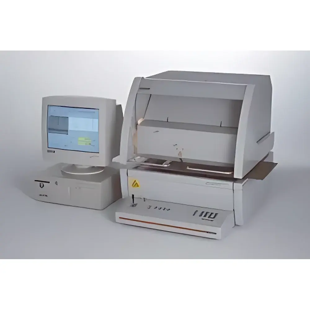
FISCHERSCOPE XDVM-W X-Ray Fluorescence Coating Thickness Analyzer
| Brand | Fischer |
|---|---|
| Origin | Germany |
| Model | XDVM-W |
| Measurement Principle | X-ray fluorescence (XRF) |
| Standards Compliance | DIN 50987, ISO 3497, ASTM B568 |
| Cabinet Dimensions (H×W×D) | 720 × 660 × 950 mm |
| Weight | ~135 kg |
| Internal Chamber (H×W×D) | 160 × 560 × 530 mm |
| X-ray Tube | Adjustable high voltage (30/40/50 kV), current up to 0.8 mA |
| Detector | Xenon-filled proportional counter with 4096-channel ADC (displayed as 256-channel spectrum) |
| Collimator Options | Standard Set I (0.1 mm, 0.2 mm, 0.05×0.05 mm², 0.03×0.2 mm² slot), optional Sets II & III |
| XY Stage Travel | 250 × 250 mm (XDVM-W standard configuration) |
| Z-axis Travel | 145 mm |
| Camera | High-resolution color CCD with dual magnification (×40 / ×80), crosshair + metric grid + spot size indicator |
| Software Platform | Native Win32 application for Windows 2000 and later |
| Language Support | English, German, French, Italian, Spanish, Chinese, Japanese |
| Data Interface | RS-232 serial port, remote command control via script files or network environment |
| Calibration | Automated beam centering, “Application Toolbox” with calibration standards and parameter disk |
| Reporting | User-defined report editor with embedded images (BMP), company logos, charts, font selection |
| Statistical Tools | SPC charts, probability plots, histogram analysis |
| Security | Customizable “short menu” lockout for critical system functions |
Overview
The FISCHERSCOPE XDVM-W is a high-precision, benchtop X-ray fluorescence (XRF) coating thickness analyzer engineered for non-destructive, quantitative measurement of metallic and alloyed layers on conductive and non-conductive substrates. Operating on the fundamental principle of energy-dispersive XRF, the instrument excites characteristic secondary (fluorescent) X-rays from elements in the sample using a micro-focused primary X-ray beam. The emitted spectral lines are resolved by a xenon-filled proportional counter and processed through a 4096-channel analog-to-digital converter—ensuring high spectral resolution and low detection limits across the elemental range from titanium (Ti, Z=22) to uranium (U, Z=92). Designed for industrial quality control laboratories and electroplating production environments, the XDVM-W meets internationally recognized metrological standards including DIN 50987, ISO 3497, and ASTM B568—making it suitable for auditable, GLP-compliant reporting in automotive, aerospace, electronics, and PCB manufacturing.
Key Features
- Motor-driven XYZ positioning system: Fully programmable 250 × 250 mm XY stage with 145 mm Z-axis travel enables precise, repeatable positioning of complex geometries—including connectors, lead frames, and multi-layer PCBs.
- Dual collimator sets: Standard Set I includes four apertures optimized for fine-feature analysis (e.g., 0.05 × 0.05 mm² square and 0.03 × 0.2 mm² slit); optional Sets II and III provide expanded flexibility for high-throughput or deep-cavity applications.
- Automated beam alignment: Real-time crosshair calibration ensures accurate targeting even on sub-millimeter features—critical for measuring solder bumps, gold fingers, or Ni/Pd/Au stacks.
- High-resolution imaging: Integrated color CCD camera with ×40/×80 optical zoom, overlay grid, and dynamic spot size indication supports visual verification prior to measurement and post-analysis documentation.
- Robust mechanical architecture: Reinforced steel cabinet (135 kg) with upward-swinging hinged door and large access chamber (560 × 530 mm internal footprint) accommodates bulky or irregularly shaped parts without re-fixturing.
- Multi-layer and alloy analysis capability: Simultaneously quantifies thickness and composition for up to three-layer systems—including cases where an alloy layer resides as outer, middle, or base layer—and resolves up to four-element alloys (e.g., Sn-Pb, Cu-Zn-Ni, Au-Ag-Cu-Pd).
Sample Compatibility & Compliance
The XDVM-W accepts a broad spectrum of sample types: rigid printed circuit boards, stamped metal components, threaded fasteners, semiconductor lead frames, and electroplated jewelry substrates. Its top-down irradiation geometry eliminates shadowing effects common in side-entry configurations, while the adjustable high-voltage X-ray tube (30–50 kV) and selectable filters (Ni, Be) optimize excitation efficiency for light elements (e.g., Al, Si, P) and heavy metals (e.g., Au, Pt, Pb) alike. All measurements adhere to traceable reference standards included in the Application Toolbox—a validated set comprising certified calibration foils and software-parameter templates. Full compliance with ISO/IEC 17025 requirements is supported via audit-ready calibration logs, user access controls, and electronic signature options compatible with FDA 21 CFR Part 11 when deployed in regulated GMP environments.
Software & Data Management
The native Win32 application provides a modular, intuitive interface supporting multilingual operation (English, German, French, Italian, Spanish, Chinese, Japanese). Measurement workflows are structured around reusable application files—each encapsulating spectral acquisition parameters, display settings, print templates, and metadata notes. Applications can be linked hierarchically to reduce redundant setup steps during batch testing. Statistical process control (SPC) tools include real-time X-bar/R charts, normal probability plots, and histogram-based capability analysis (Cp/Cpk). Data export supports RS-232 serial transmission for integration into MES or LIMS platforms; remote operation is enabled via ASCII command scripts executed over local network or direct serial connection. Reports—generated with embedded BMP images, corporate branding, and customizable formatting—are exportable to .DOC format for archival or regulatory submission.
Applications
This system delivers quantitative performance in high-volume manufacturing contexts where layer integrity directly impacts functional reliability. Typical use cases include: thickness verification of ENIG (electroless nickel immersion gold) finishes on PCB pads; compositional analysis of ternary brass (Cu-Zn-Sn) plating on automotive terminals; measurement of Cr(VI)-free trivalent chromium coatings on zinc die-cast housings; quantification of Pd/Ni underlayers beneath wire-bondable Au caps; and monitoring of electrolyte bath composition via direct solution analysis (up to two metal ions). Its ability to resolve overlapping peaks—such as Cu Kα and Ni Kβ—through advanced deconvolution algorithms ensures accuracy in complex multilayer stacks encountered in MEMS packaging and RF shield deposition.
FAQ
What is the minimum measurable layer thickness?
Detection limits depend on element pair, matrix, and measurement time—but typical single-layer detection thresholds range from 0.01 µm (for high-Z elements like Au on Cu) to 0.1 µm (for light elements such as Al on Si).
Can the system analyze plated-through holes (PTHs) in PCBs?
Yes—using the optional collimator Set III (0.025 × 0.025 mm² aperture) and Z-axis auto-focus, the instrument achieves reliable signal acquisition from sidewalls and bottom surfaces of deep vias.
Is method validation support available per ISO 17025?
Fischer provides documented uncertainty budgets, linearity studies, and repeatability/reproducibility (R&R) test protocols upon request—fully aligned with ILAC-G8 and EURACHEM guidelines.
How is calibration maintained over time?
The system supports scheduled recalibration using traceable reference standards; drift correction is performed automatically via internal reference peak monitoring during routine operation.
Does the software comply with FDA 21 CFR Part 11 requirements?
When configured with password-protected user roles, electronic signatures, and full audit trail logging (including all parameter changes and measurement deletions), the XDVM-W software satisfies core Part 11 technical controls for electronic records and signatures.


