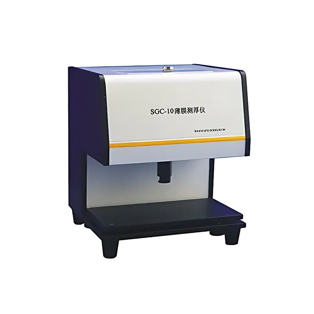
KJ GROUP SGC-10 White-Light Interferometric Thin-Film Thickness Metrology System
| Brand | KJ GROUP (Shenyang Kejing) |
|---|---|
| Origin | Liaoning, China |
| Manufacturer Type | Authorized Distributor |
| Country of Origin | China |
| Model | SGC-10 |
| Pricing | Upon Request |
| Measurement Principle | White-Light Interferometry |
| Thickness Range | 20 nm – 50 µm (thickness-only mode) |
| Accuracy | <1 nm or <0.5% |
| Repeatability | 0.1 nm |
| Spectral Range | 380–1000 nm |
| Max. Layers | 4 |
| Spot Diameter | Adjustable from 1.2 mm to 10 mm |
| Minimum Measurable Area | Ø ≥ 1.2 mm |
| Measurement Time | 5–60 s per acquisition |
| Light Source | Long-life tungsten-halogen lamp (2000 h lifetime) |
| Detector | Imported fiber-coupled miniature spectrometer |
| Fiber | UV-VIS-NIR grade fused silica optical fiber |
| Sample Stage | 290 mm × 160 mm |
| Power Supply | AC 110–240 V, 50–60 Hz |
| Dimensions | 300 mm × 300 mm × 350 mm |
| Weight | 18 kg |
Overview
The KJ GROUP SGC-10 White-Light Interferometric Thin-Film Thickness Metrology System is a precision optical metrology instrument engineered for non-destructive, contactless characterization of thin-film structures in R&D and production environments. It operates on the physical principle of white-light interferometry—analyzing spectral interference fringes generated by coherent superposition of light reflected from the film surface and the film-substrate interface. By fitting the measured reflectance spectrum against theoretical models based on Fresnel equations and thin-film optics, the system quantitatively retrieves layer thickness (d), refractive index (n), and extinction coefficient (k) for up to four stacked layers simultaneously. Designed in technical collaboration with New-Span Inc. (USA), the SGC-10 integrates a high-stability broadband illumination source, a compact fiber-coupled spectrometer, and a modular optical probe architecture—enabling both benchtop and microscope-integrated configurations for micro-area analysis.
Key Features
- Non-contact, non-invasive measurement using fiber-optic probe—eliminates risk of sample damage, contamination, or mechanical drift;
- Simultaneous determination of thickness, n, and k for single-layer and multilayer stacks (up to 4 layers) in a single acquisition cycle;
- Adjustable spot size (1.2–10 mm diameter) optimized for macro- and micro-scale measurements—compatible with C-mount microscope integration for localized analysis down to ~10 µm resolution;
- Embedded miniature fiber-optic spectrometer (380–1000 nm range) with UV-VIS-NIR-grade fused silica fiber for high signal fidelity and long-term spectral stability;
- High repeatability (±0.1 nm) and accuracy (<1 nm or <0.5%, whichever is greater) validated across SiO₂, SiNₓ, ITO, photoresists, and polymer dielectrics;
- Modular hardware design: detachable probe and standardized fiber interface allow flexible deployment in cleanrooms, gloveboxes, or integrated process tools;
- Long-life tungsten-halogen broadband source (rated >2000 h) ensures consistent spectral output without recalibration drift;
- Robust mechanical platform with 290 mm × 160 mm motorized or manual sample stage supporting wafers, glass substrates, and flexible films.
Sample Compatibility & Compliance
The SGC-10 supports transparent, semi-transparent, and weakly absorbing thin films deposited on optically contrasting substrates—including silicon, fused silica, sapphire, BK7 glass, and metal-coated carriers. It is routinely deployed for quality control of antireflection coatings, OLED encapsulation layers, MEMS passivation films, semiconductor gate dielectrics (e.g., HfO₂, Al₂O₃), and liquid crystal alignment layers. While not certified to ISO/IEC 17025 or ASTM E2581 out-of-the-box, the system’s traceable calibration methodology, audit-ready data export (CSV, XML, .tdms), and timestamped measurement logs align with GLP and internal GMP documentation requirements. Software-generated reports include full spectral raw data, model residuals, confidence intervals for fitted parameters, and user-defined metadata fields—facilitating regulatory review under FDA 21 CFR Part 11 when paired with institutional electronic signature protocols.
Software & Data Management
The proprietary MetroFilm™ analysis suite provides a deterministic, physics-based fitting engine grounded in rigorous thin-film optical modeling. It includes an expandable material database containing >120 pre-characterized optical constants (n, k vs. λ) for common inorganic, organic, and metallic thin-film materials—curated from peer-reviewed literature and NIST databases. Users may import custom dispersion models (Sellmeier, Cauchy, Tauc-Lorentz) or define empirical n/k tables. The software supports batch processing of multi-point maps, statistical thickness uniformity analysis (within-wafer, wafer-to-wafer), and automated pass/fail thresholding against specification limits. All measurement sessions are archived with full parameter history, including ambient temperature, lamp intensity, and fiber coupling efficiency—ensuring full experimental reproducibility. Export formats comply with ASTM E2581 Annex A1 for optical thin-film metrology reporting.
Applications
- Process development and endpoint detection in PVD, CVD, ALD, and spin-coating lines;
- Failure analysis of delamination, interfacial oxidation, or stoichiometric drift in functional coatings;
- Optical design validation of multilayer interference filters and beam splitters;
- Thickness uniformity mapping across 4-inch and 6-inch wafers;
- Characterization of gradient-index films and graded-composition stacks;
- Support for DOE-driven optical coating optimization and machine-learning–assisted inverse design workflows.
FAQ
What substrates are compatible with the SGC-10?
Silicon, quartz, sapphire, BK7, fused silica, stainless steel, and aluminum substrates are supported—provided sufficient optical contrast exists between film and substrate in the 380–1000 nm range.
Can the system measure absorbing films like metals or doped oxides?
Yes—within its operational thickness and absorption constraints. For highly absorbing films (e.g., Cr, Ti, NiCr), accurate k extraction requires careful modeling of surface roughness and native oxide contributions.
Is microscope integration mandatory for micro-area measurement?
No—micro-area capability is optional. The standard probe delivers 1.2 mm spot size; C-mount adapter enables coupling to third-party upright or inverted microscopes for sub-50 µm spatial resolution.
Does the software support scripting or API access for automation?
The MetroFilm™ platform offers COM automation interface (Windows) and Python-compatible DLL wrappers for integration into LabVIEW, MATLAB, or custom MES/SCADA systems.
How often does the system require recalibration?
Under stable environmental conditions (±1 °C, low vibration), annual verification using NIST-traceable SiO₂-on-Si reference standards is recommended. Lamp intensity drift is self-compensated via internal reference channel normalization.
Related Products


