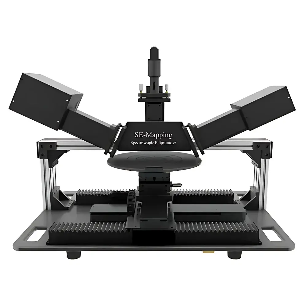
KJ GROUP SE-Mapping Spectroscopic Ellipsometer
| Brand | KJ GROUP |
|---|---|
| Origin | Liaoning, China |
| Manufacturer Type | Authorized Distributor |
| Country of Origin | China |
| Model | SE-Mapping |
| Price | Upon Request |
| Light Source | Deuterium + Tungsten-Halogen (193–2500 nm) |
| Measurement Modes | Ψ/Δ, n/k, R/T spectra |
| Incidence Angle | Fixed at 65° |
| Spot Size | 2–3 mm (macro), 200 µm (micro) |
| Mapping Range | 300 × 300 mm |
| Sample Max Diameter | 300 mm |
| Measurement Time per Point | 0.5–5 s |
| Thickness Repeatability | ±0.01 nm |
| Focus Method | Manual |
| Optical Configuration | PCRSA (Photoelastic Modulator-based Compensator Rotating System Architecture) |
| Optional Accessories | Vacuum Pump, Transmission Adsorption Module |
Overview
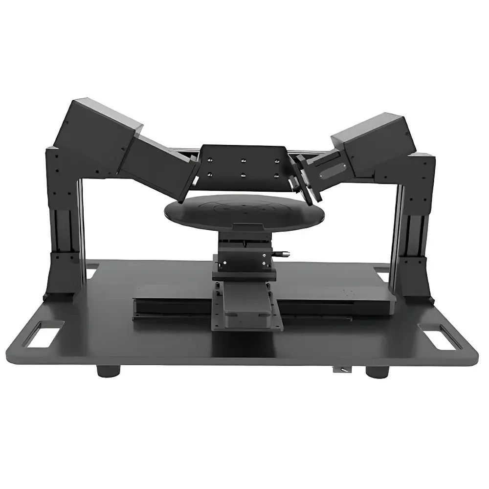
The KJ GROUP SE-Mapping Spectroscopic Ellipsometer is a precision metrology instrument engineered for non-contact, non-destructive characterization of thin-film optical properties across full wafers or large-area substrates. Operating on the fundamental principle of spectroscopic ellipsometry—measuring the change in polarization state (Ψ and Δ) of light reflected from a sample surface—the system quantifies complex refractive index (n, k), film thickness, interfacial roughness, and compositional gradients with sub-nanometer resolution. Unlike point-measurement ellipsometers, the SE-Mapping integrates a motorized XYZ stage and high-stability optical head to execute spatially resolved, automated spectroscopic mapping over areas up to 300 × 300 mm. Its dual-lamp illumination (deuterium lamp for UV, tungsten-halogen for Vis–NIR) delivers continuous spectral coverage from 193 nm to 2500 nm, enabling accurate modeling of wide-bandgap semiconductors, transparent conductive oxides, organic layers, and multilayer stacks encountered in advanced optoelectronic manufacturing.
Key Features
- Full-wafer spectroscopic mapping capability with programmable grid definition, step size control, and auto-alignment routines for repeatable spatial sampling.
- PCRSA optical architecture—combining photoelastic modulator (PEM) compensation with rotating analyzer detection—ensures high signal-to-noise ratio and rapid acquisition of Ψ/Δ spectra (0.5–5 s per measurement point).
- Dual broadband light source (193–2500 nm) supports unified modeling of UV-absorbing materials (e.g., SiNx, AlGaN) and NIR-transparent films (e.g., ITO, SiO2) without hardware reconfiguration.
- Two-spot optical configuration: macro-spot (2–3 mm diameter) for rapid uniformity screening; micro-spot (200 µm) for localized defect analysis or patterned device interrogation.
- Fixed-angle incidence geometry (65°) optimized for high sensitivity to thickness and dielectric function in single- and multi-layer dielectric stacks.
- Modular software framework enabling OEM-level customization of measurement sequences, report templates, and integration with factory automation protocols (SECS/GEM, OPC UA).
Sample Compatibility & Compliance
The SE-Mapping accommodates rigid planar substrates up to 300 mm in diameter—including silicon wafers, glass panels (Gen 2–Gen 6), quartz carriers, and metal-coated foils—with vacuum chuck or mechanical clamping options. Optional transmission adsorption modules extend functionality to semi-transparent or freestanding membranes. All measurement workflows adhere to principles outlined in ASTM E1938 (Standard Guide for Spectroscopic Ellipsometry), ISO 15382 (Thin film thickness measurement by ellipsometry), and support GLP-compliant data integrity through audit-trail-enabled session logging. While not FDA-certified as standalone medical device hardware, the system’s raw data export (ASCII, CSV, SOP-compatible XML) and metadata-rich file structure facilitate compliance with 21 CFR Part 11 requirements when deployed within validated laboratory information management systems (LIMS).
Software & Data Management
The proprietary EllipsoMap™ software provides a unified interface for instrument control, real-time spectral visualization, and physics-based regression analysis. It embeds over 300 pre-validated material dispersion models (Cauchy, Tauc-Lorentz, Cody-Lorentz, B-Spline) and supports user-defined layer stack definitions with graded interfaces, roughness zones, and anisotropic dielectric tensors. Batch processing enables parallel fitting of hundreds of map points using identical optical models, with convergence diagnostics and uncertainty propagation reported per pixel. Export formats include TIFF-based thickness heatmaps, CSV spectral libraries, and PDF summary reports containing statistical metrics (mean, σ, min/max, CV%) across user-defined regions of interest (ROIs). Data files are timestamped, digitally signed, and retain full traceability to instrument configuration, calibration history, and environmental logs.
Applications
- OLED and micro-LED display manufacturing: thickness uniformity mapping of HTL/ETL emissive layers (e.g., NPB, Alq3, quantum dots) on TFT backplanes.
- Photovoltaic R&D and production: inline monitoring of anti-reflective coatings (SiNx, TiO2), passivation layers (Al2O3, SiOx), and tandem cell absorbers (perovskite/Si).
- Semiconductor process control: metrology of high-k gate dielectrics (HfO2, ZrO2), low-k interlayer dielectrics (SiCOH), and epitaxial III–V films.
- Optical coating QA: verification of spectral reflectance/transmittance profiles and stress-induced birefringence in AR/HR filters.
- Research on 2D materials: determination of layer count, stacking order, and substrate-induced doping in graphene, MoS2, and h-BN heterostructures.
FAQ
What spectral range is standard, and can it be extended?
The base configuration covers 193–2500 nm using synchronized deuterium and tungsten-halogen sources. No hardware modification is required for full-range operation.
Is the 65° incidence angle adjustable?
No—the optical head is mechanically fixed at 65° to ensure thermal and mechanical stability during long-duration mapping runs. Custom incidence angles are available under OEM collaboration agreements.
How is focus maintained across large-area maps?
Manual coarse focus is performed prior to mapping; Z-axis repeatability is ±0.5 µm over the full travel range. For warped or bowed substrates, optional laser triangulation autofocus can be integrated.
Does the system support vacuum or inert-atmosphere measurements?
Yes—vacuum pump integration (optional accessory) enables measurements under ≤10⁻³ mbar, critical for air-sensitive perovskites or reactive metal oxides.
Can measurement data be exported for third-party modeling tools?
Yes—raw Ψ/Δ spectra, fitted parameters, and coordinate metadata are exportable in ASCII, CSV, and HDF5 formats compatible with MATLAB, Python (NumPy/SciPy), and commercial TCAD platforms.


