Mask Template for Thin-Film Deposition Systems
| Brand | KJ GROUP (Shenyang Kejing) |
|---|---|
| Origin | Liaoning, China |
| Manufacturer Type | Authorized Distributor |
| Country of Origin | China |
| Model | Custom Mask Template |
| Pricing | Upon Request |
Overview
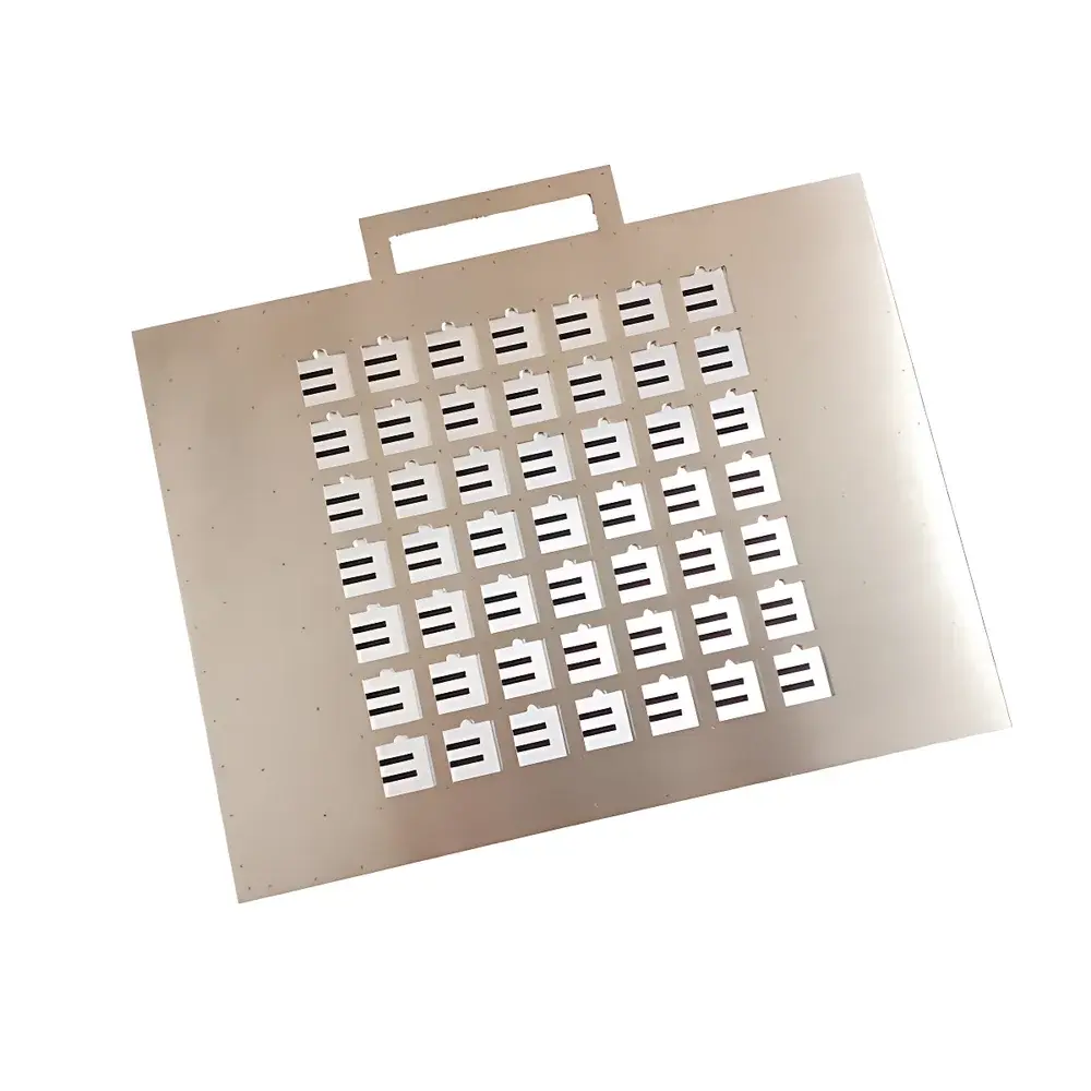
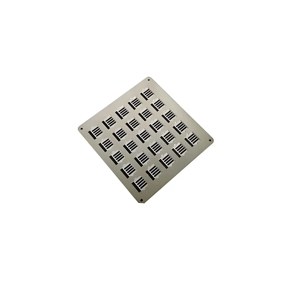
Custom mask templates are precision-engineered photolithographic or physical vapor deposition (PVD) auxiliary components designed for spatially selective thin-film patterning in vacuum-based coating systems. These masks function as physical stencils placed between the evaporation source and substrate, enabling controlled material deposition only in defined geometric regions. Unlike photomasks used in optical lithography, these templates operate under high-vacuum conditions (typically 10−5–10−7 Torr) and are compatible with thermal evaporation, electron-beam evaporation, and sputtering processes. Their primary role is to achieve micron-level pattern fidelity without requiring photoresist processing—making them ideal for rapid prototyping, R&D-scale device fabrication, and multi-layer alignment in academic and industrial thin-film laboratories.
Key Features
- Substrate-grade 304 or 316 stainless steel construction, offering high dimensional stability, low outgassing rates (<1×10⁻¹⁰ Torr·L/s·cm²), and resistance to thermal cycling up to 300 °C in vacuum environments
- Fabricated via CNC micromachining or laser ablation to ensure edge roughness <±0.5 µm and positional tolerance ≤±2 µm across apertures
- Flatness maintained at ≤2 µm over 100 mm span, verified by optical interferometry prior to shipment
- Optional surface passivation (electropolishing or TiN coating) available to minimize particle shedding and enhance corrosion resistance during reactive sputtering
- Compatible with standard KF-40, CF-63, or ISO-K 160 flange mounting configurations for integration into common benchtop and production-scale deposition chambers
Sample Compatibility & Compliance
KJ GROUP custom mask templates support substrates up to 6 inches (150 mm) in diameter and accommodate aperture dimensions ranging from 50 µm to 20 mm. Each template is fabricated per customer-provided DXF or Gerber layout files, with design review conducted to verify manufacturability, aspect ratio constraints (max 10:1 for thickness:aperture width), and thermal shadowing effects. Templates comply with ISO 14644-1 Class 5 cleanroom handling protocols during final inspection and packaging. Documentation includes a Certificate of Conformance (CoC) listing material lot traceability, surface roughness measurements (Ra <0.2 µm), and vacuum bake-out test results (24 h at 150 °C, pressure rise <5×10⁻⁸ Torr).
Software & Data Management
While mask templates are passive hardware components, KJ GROUP provides full digital traceability through its integrated order management system. Customers receive encrypted access to native CAD files (STEP/IGES), coordinate measurement machine (CMM) reports, and metrology certificates via secure portal download. All design data adheres to ISO 10303-21 (STEP AP242) standards to ensure interoperability with industry-standard simulation tools such as COMSOL Multiphysics® and ANSYS® for deposition uniformity modeling. For regulated environments, audit logs—including revision history, operator ID, and timestamped inspection records—are retained for ≥10 years in accordance with GLP and ISO/IEC 17025 requirements.
Applications
- Pre-patterned electrode fabrication for organic light-emitting diodes (OLEDs) and perovskite solar cells
- Multi-step metallization in MEMS sensor development (e.g., Au/Cr contact pads, Al interconnects)
- Gradient film studies requiring graded aperture arrays for compositional control
- Calibration reference structures in sheet resistance mapping and Hall effect characterization
- Mask alignment verification using fiducial markers for sequential layer deposition (e.g., top-gate OTFTs)
FAQ
What minimum feature size can be reliably fabricated?
Standard capability is 50 µm; sub-30 µm features require consultation due to aspect ratio and shadowing limitations.
Do you provide alignment aids or registration marks?
Yes—crosshair fiducials, vernier scales, and laser-etched alignment notches are included at no additional cost upon request.
Can masks be reused across multiple deposition runs?
Yes, provided they undergo proper cleaning (acetone/IPA ultrasonication) and visual inspection for aperture deformation or particulate accumulation before each use.
Is electroplating or Ni coating available for enhanced durability?
Nickel electroplating (5–8 µm thickness) and DLC (diamond-like carbon) coating options are available for extended service life in aggressive plasma environments.
How long is the typical lead time for custom designs?
Standard turnaround is 12–15 business days from approved drawing; expedited fabrication (7-day delivery) is offered with priority scheduling.
Related Products


