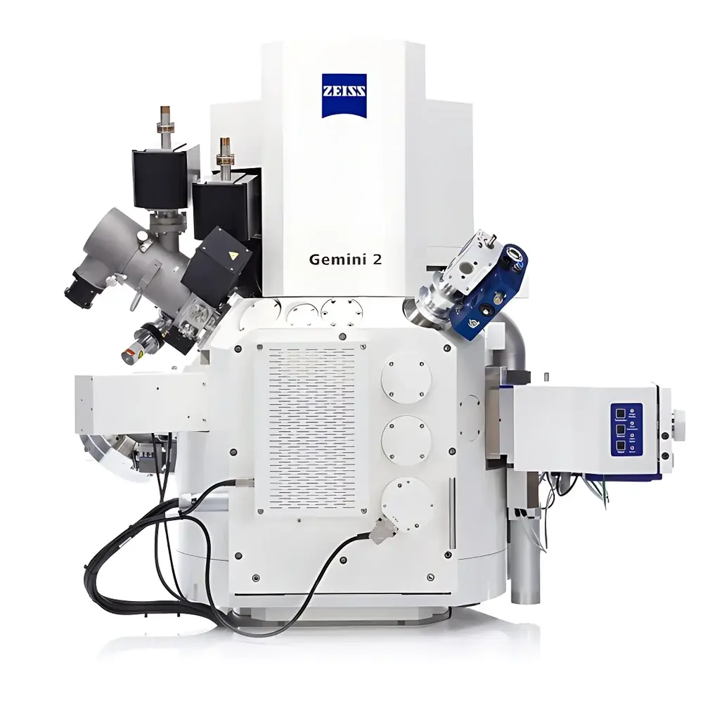
ZEISS Crossbeam Series FIB-SEM DualBeam Microscope
| Brand | ZEISS |
|---|---|
| Origin | Germany |
| Instrument Type | Floor-standing DualBeam System |
| Electron Source | Thermal Field Emission Gun |
| Secondary Electron Resolution | 0.9 nm @ 15 kV (Crossbeam 550), 1.0 nm @ 15 kV (Crossbeam 340) |
| Magnification Range | 12× – 2,000,000× (SEM mode) |
| Acceleration Voltage | 0.02–30 kV (SEM), 0.5–30 kV (FIB) |
| Backscattered Electron Resolution | Not specified |
Overview
The ZEISS Crossbeam Series is a high-precision floor-standing FIB-SEM DualBeam microscope engineered for correlative nanoscale imaging, in situ nanofabrication, and high-throughput 3D structural and compositional analysis. Integrating a thermal field emission scanning electron microscope (FE-SEM) column with a gallium liquid metal ion source (LMIS) focused ion beam (FIB) column in a single vacuum chamber, the system enables simultaneous or sequential electron imaging, ion milling, deposition, and gas-assisted etching. Its coaxial beam geometry and ultra-stable mechanical architecture ensure sub-nanometer spatial registration between SEM and FIB coordinates—critical for iterative lift-out, site-specific TEM lamella preparation, and serial sectioning workflows. Designed and manufactured in Oberkochen, Germany, the Crossbeam platform adheres to ISO 9001-certified production standards and is validated for use in GLP-compliant laboratories and ISO/IEC 17025-accredited testing facilities.
Key Features
- Thermal field emission electron source delivering high brightness and long-term stability at low accelerating voltages (down to 200 V), enabling high-resolution imaging of beam-sensitive and non-conductive specimens without charge compensation layers.
- Coaxial FIB-SEM alignment with <10 nm positional repeatability, supporting true “see-while-cut” operation via real-time secondary electron monitoring during ion milling.
- Integrated Atlas 5 software suite for automated multi-scale, multi-modal image acquisition—including stitching, drift correction, and synchronized SEM/FIB scripting—enabling reproducible large-area mapping and serial block-face imaging.
- Modular architecture supporting field-upgradable hardware options: time-of-flight secondary ion mass spectrometry (ToF-SIMS) for 3D chemical tomography; femtosecond laser ablation module for rapid sub-millimeter trenching and bulk material removal with minimal thermal damage and chamber contamination.
- Patented magnetic-free electron column design eliminates Lorentz force interference on ion trajectories, ensuring consistent milling accuracy across extended dwell times and complex pattern sequences.
- Automated TEM lamella preparation workflow compliant with ASTM E2821–22 guidelines for electron-transparent specimen generation, including thickness monitoring via electron channeling contrast and in situ lift-out validation.
Sample Compatibility & Compliance
The Crossbeam accommodates diverse sample geometries—from 4-inch wafers and 30 mm SEM stubs to irregularly shaped bulk materials—via motorized 5-axis stage with ±90° tilt and 360° rotation. Non-conductive samples (e.g., polymers, biological tissues, ceramics) are imaged stably under low-kV conditions (<2 kV) without sputter coating, leveraging beam deceleration and optimized detector biasing. The system meets electromagnetic compatibility requirements per EN 61326-1 and operates within Class 1000 cleanroom specifications when equipped with optional vibration isolation and hydrocarbon-free pumping. All software-controlled operations comply with FDA 21 CFR Part 11 for audit trail logging, electronic signatures, and data integrity assurance—fully traceable for GMP-regulated semiconductor and medical device R&D environments.
Software & Data Management
Acquisition, processing, and reporting are unified under ZEISS SMART and ZEN Connect platforms. Atlas 5 provides scriptable automation for batch TEM lamella prep, serial sectioning (SBF-SEM), and region-of-interest (ROI) targeting based on machine-learning-assisted feature recognition. Raw data—including SE, BSE, EDS, EBSD, and ToF-SIMS hyperspectral cubes—is stored in vendor-neutral HDF5 format with embedded metadata (acquisition parameters, calibration timestamps, user annotations). Integration with Thermo Fisher Velox, Oxford AZtec, and Bruker Esprit enables cross-platform EDS/EBSD correlation. All datasets support FAIR principles (Findable, Accessible, Interoperable, Reusable) and export to standardized formats (TIFF, MRC, NRRD) for third-party reconstruction (e.g., IMOD, Amira, Dragonfly).
Applications
- Materials Science: Crystallographic orientation mapping (EBSD), grain boundary characterization, nanopore fabrication in MOFs, and in situ micromechanical testing using integrated nanoindenter modules.
- Semiconductor & IC Failure Analysis: Circuit edit via Pt/C deposition, cross-sectioning of FinFETs and GAA transistors, backside FIB milling through Si substrates, and 3D NAND stack tomography with layer-by-layer segmentation.
- Battery Research: Quantitative porosity and tortuosity analysis in cathode/anode composites, solid-electrolyte interphase (SEI) thickness profiling, and post-cycling particle fracture mapping.
- Life Sciences: Correlative light-electron microscopy (CLEM) workflows, serial section TEM of neural tissue (e.g., C. elegans connectomics), and cryo-FIB milling of vitrified cells for high-resolution structural biology.
- Geosciences & Metallurgy: Inclusion phase identification in superalloys, corrosion pit depth profiling, and interface diffusion analysis at metal/ceramic junctions.
- Advanced Manufacturing: Nanofluidic channel fabrication in silicon/glass, micro-optical element patterning, and atom probe tomography (APT) tip sharpening with sub-50 nm apex radius control.
FAQ
What vacuum levels are maintained in the SEM and FIB columns?
The electron column operates at ≤1 × 10⁻⁷ mbar; the ion column maintains ≤5 × 10⁻⁸ mbar during milling—achievable via differential pumping and cold traps.
Is the system compatible with cryogenic stages for beam-sensitive samples?
Yes—optional cryo-transfer holders and LN₂-cooled stages are available and certified for use down to −180 °C.
Can the Crossbeam be integrated into automated lab infrastructure?
It supports SECS/GEM communication protocols and offers RESTful API access for integration with MES, LIMS, and robotic sample handling systems.
How is beam damage minimized during serial sectioning?
Through adaptive dwell time control, low-dose imaging modes, and real-time dose monitoring integrated into Atlas 5’s sectioning scheduler.
What certification documentation is provided for regulatory submissions?
Each system ships with Factory Acceptance Test (FAT) report, IQ/OQ documentation templates, and traceable calibration certificates aligned with ISO/IEC 17025 requirements.


