Appo NIL-100 4-Inch Nanoimprint Lithography System
| Brand | Appo |
|---|---|
| Origin | Shanghai, China |
| Model | NIL-100 |
| Imprint Area | 4-inch (100 mm) wafers/substrates |
| Max. Pressure | 8 bar (integrated air compressor), 20 bar (external cleanroom supply) |
| Temperature Range | Ambient to 250 °C |
| UV Source | 400 W high-pressure Hg lamp, dominant wavelength 365 nm |
| Vacuum Level | ≤10 Pa |
| Heating Method | Electromagnetic single-side heating |
| Automation | Motorized auto-demolding |
| Compatible imprint modes | Thermal embossing & UV-curable step-and-flash imprint lithography (S-FIL) |
| Optional consumables | Full suite of nanoimprint resists (thermal, UV-curable, lift-off, deep-etch), anti-sticking agents, adhesion promoters, and custom mold fabrication support (Ni, SFP®, Hybrid Mold®) |
| Resolution capability | ≤20 nm (with appropriate mold and process optimization) |
| Compliance | Designed for R&D and pilot-line use under GLP-aligned lab practices |
Overview
The Appo NIL-100 is a dual-mode, 4-inch nanoimprint lithography (NIL) system engineered for precision nanofabrication in academic research laboratories and semiconductor pilot facilities. It implements two fundamentally distinct imprint mechanisms—thermal embossing and ultraviolet (UV) step-and-flash imprint lithography (S-FIL)—within a single, integrated platform. Unlike optical or electron-beam lithography, NIL relies on direct mechanical pattern transfer from a master mold into a thin polymer resist layer, bypassing diffraction limits and enabling sub-20 nm feature resolution over large areas without complex optics or vacuum electron columns. The NIL-100’s architecture integrates vacuum-assisted cavity evacuation (<10 Pa), programmable temperature control (ambient to 250 °C), regulated pressure application (up to 20 bar), electromagnetic single-side heating, and broadband UV exposure (365 nm, 400 W Hg lamp), all coordinated through a deterministic PLC-based control system with a responsive HMI interface. Its design emphasizes reproducibility, mold longevity, and process transparency—critical for method development, technology transfer, and regulatory-compliant documentation.
Key Features
- Dual-mode operation: Simultaneous support for thermal embossing (using thermoplastic resists such as PMMA) and UV-curable S-FIL (employing low-viscosity monomer formulations)
- 4-inch substrate compatibility: Optimized for standard 100 mm wafers, glass slides, flexible polymer films (PET, PC, PI), and curved substrates (e.g., optical fibers)
- Precision environmental control: Vacuum chamber with ≤10 Pa base pressure; closed-loop temperature regulation from ambient to 250 °C; pressure control up to 20 bar via external cleanroom supply
- Electromagnetic single-side heating: Enables rapid, uniform thermal ramping with minimal thermal lag—critical for glass transition control in thermoplastic imprinting
- Motorized auto-demolding: Reduces shear-induced pattern damage and improves throughput consistency during mold separation
- Integrated UV exposure module: 400 W high-pressure mercury lamp with primary emission at 365 nm, calibrated for uniform irradiance across the imprint field
- Modular consumables ecosystem: Includes thermally stable resists, UV-curable monomers, lift-off-compatible resists, deep-etch resists, anti-stiction coatings, and substrate adhesion promoters
- Custom mold integration: Supports rigid Ni templates, soft SFP® and Hybrid Mold® elastomeric stamps, and hybrid rigid-soft architectures for defect-tolerant imprinting
Sample Compatibility & Compliance
The NIL-100 accommodates a broad range of substrate materials—including silicon, fused silica, quartz, sapphire, ITO-coated glass, PET, PMMA, polyimide, and metal foils—as well as non-planar geometries such as cylindrical optical fibers. Its vacuum-sealed chamber and low-residue demolding strategy minimize particle entrapment, while optional anti-stiction treatments enable high-yield release from high-aspect-ratio features. From a compliance perspective, the system is configured for GLP-aligned operation: all process parameters (temperature setpoint, pressure profile, UV dose, vacuum decay rate, dwell time) are timestamped and logged in machine-readable format. While not certified for GMP production, its deterministic control architecture and audit-trail-capable software facilitate validation protocols required by ISO 9001, ASTM E2784 (standard guide for nanoimprint lithography), and internal QC workflows aligned with FDA 21 CFR Part 11 principles (when paired with validated third-party data management systems).
Software & Data Management
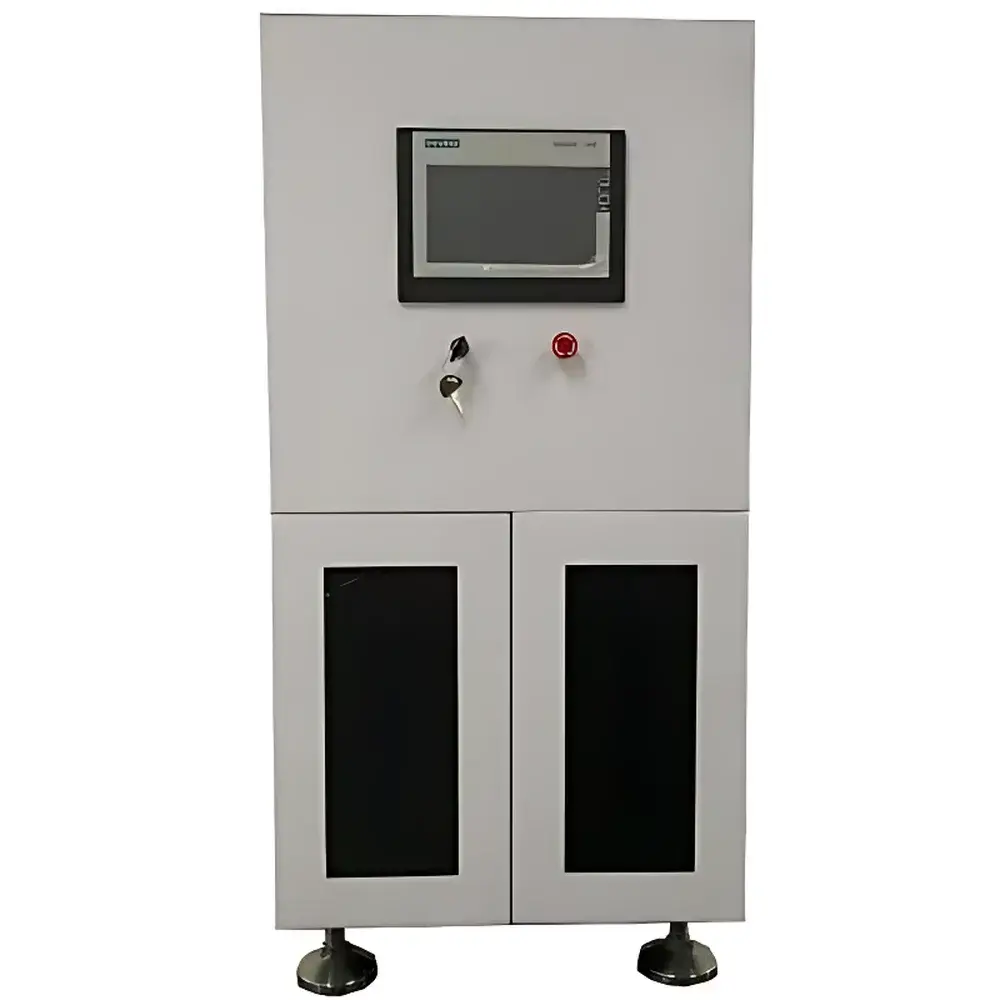
Operation is managed via an embedded industrial PLC with a 10.1-inch capacitive touchscreen HMI. The interface provides intuitive access to preloaded process recipes (e.g., “Ni-template thermal imprint on PET”, “S-FIL on SiO₂/Si”), real-time parameter visualization (pressure vs. time, T vs. t, UV intensity monitoring), and manual override controls for R&D flexibility. All executed runs generate CSV-formatted log files containing timestamps, sensor readings, actuator states, and operator annotations—enabling traceability and statistical process analysis (SPC). The system does not include proprietary cloud connectivity; however, local network export (Ethernet) allows integration with institutional LIMS or MATLAB/Python-based analysis pipelines. Firmware updates are delivered via secure USB import, ensuring version control and reproducibility across multi-user environments.
Applications
The NIL-100 serves as a foundational tool for nanoscale patterning across multiple domains: semiconductor prototyping (sub-32 nm gate structures, plasmonic metasurfaces), MEMS/NEMS device fabrication (high-aspect-ratio actuators, resonators), biochip development (nanopillar-based cell capture arrays, grating-coupled biosensors), photonic crystal fabrication (VCSEL templates, AR/VR waveguide couplers), and flexible electronics (transparent electrodes on PET, stretchable antenna patterns). Its compatibility with lift-off resists enables direct metal nanostructure definition without etch steps; its Ni-template thermal mode permits direct patterning of polymer substrates—eliminating transfer etch entirely. Curved-surface imprinting capability extends utility to fiber-optic sensing and conformal optoelectronics.
FAQ
What imprint modes does the NIL-100 support?
Thermal embossing and UV-curable step-and-flash imprint lithography (S-FIL), both fully programmable within the same hardware platform.
Can the system handle non-planar substrates?
Yes—it has been validated for imprinting on cylindrical optical fibers and other gently curved surfaces using compliant SFP® and Hybrid Mold® stamps.
Is mold cleaning or maintenance supported onboard?
No dedicated cleaning module is included; however, the vacuum chamber design and anti-stiction agent compatibility facilitate post-process solvent rinsing and plasma ashing using external tools.
What level of process documentation does the system provide?
Full parameter logging per run (time-stamped pressure, temperature, UV exposure duration/intensity, vacuum decay), exported as CSV for SPC or regulatory review.
Are custom molds supplied with the system?
Standard configurations include a 4-inch 400 nm dot-array Ni template; additional molds (including SFP®, Hybrid Mold®, and customer-specific designs) are available as optional accessories with lead-time dependent on complexity.


