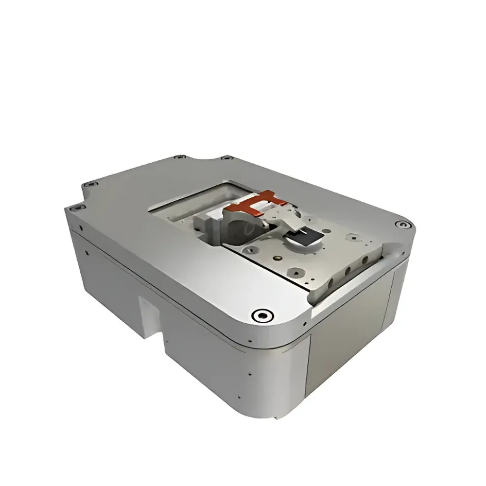
NenoVision LiteScope In-Situ Atomic Force Microscope
| Origin | Czech Republic |
|---|---|
| Manufacturer Type | Distributor |
| Origin Category | Imported |
| Model | LiteScope |
| Price Range | USD 65,000–130,000 |
| Instrument Type | Atomic Force Microscope |
| Positional Detection Noise | AFM-in-SEM Integration |
| Sample Dimensions | In-situ AFM-compatible |
| Stage Travel Range | 100 × 100 × 100 µm |
Overview
The NenoVision LiteScope is a purpose-engineered in-situ atomic force microscope (AFM) designed for seamless integration into commercial scanning electron microscopes (SEM). Unlike conventional standalone AFMs, the LiteScope operates within the SEM chamber—enabling true correlative probe-electron microscopy (CPEM). This architecture leverages simultaneous or sequential acquisition of high-resolution topographic, mechanical, electrical, and magnetic data from the *exact same region* imaged by SEM, without sample transfer or repositioning. The system employs a self-sensing cantilever design—eliminating reliance on optical beam deflection—and is engineered for operation under high vacuum (10−5 Pa) and optionally ultra-high vacuum (UHV) conditions. Its compact form factor (129 × 90 × 45–55 mm), retractable measurement head, and tilt capability (0°–60°, minimum working distance = 5 mm) ensure compatibility with diverse SEM configurations—including those equipped with focused ion beam (FIB), gas injection systems (GIS), and energy-dispersive X-ray spectroscopy (EDX) detectors.
Key Features
- True CPEM architecture: Synchronized spatial registration between SEM imaging and AFM probing at sub-100 nm alignment accuracy
- Self-sensing cantilevers: No laser alignment required; immune to chamber vibrations and optical path obstruction
- Modular probe interface: Interchangeable probe holders support AFM, STM, EFM, KPFM, MFM, FMM, and nanoindentation modes
- Rapid integration: Mounts to standard SEM stages via four screws; full mechanical and electrical connection achieved in ≤5 minutes
- Retractable head design: Minimizes physical footprint around the sample—critical for multi-technique workflows
- Environmental flexibility: Operates at ambient temperature (15–25 °C); compatible with high-vacuum (10−5–105 Pa) and UHV configurations upon request
- High-precision navigation: Real-time SEM-guided tip positioning enables targeted interrogation of sub-micron features identified in secondary electron images
Sample Compatibility & Compliance
The LiteScope accommodates samples up to 22 mm × 11 mm × 8 mm in volume, with a maximum lateral scan range of 100 µm × 100 µm and vertical range of 100 µm. Its non-optical detection scheme eliminates constraints imposed by chamber window transmission or stage height clearance—making it suitable for irregular, tilted, or coated specimens. The system complies with ISO/IEC 17025 requirements for measurement traceability when used with calibrated reference samples (e.g., Si grating standards, NIST-traceable roughness standards). While not certified for GLP/GMP environments out-of-the-box, its software supports audit trails, user access control, and electronic signatures—facilitating compliance with FDA 21 CFR Part 11 when deployed in regulated laboratories.
Software & Data Management
LiteScope Control Software provides unified control of both SEM navigation and AFM acquisition through a single GUI. It supports real-time overlay of AFM topography onto SEM frames, enabling pixel-registered correlative analysis. All raw data—including force-distance curves, current maps, phase signals, and Kelvin potential distributions—are stored in HDF5 format with embedded metadata (timestamp, probe ID, calibration parameters, vacuum pressure, stage coordinates). Remote access is enabled via secure SSH tunneling or VPN-authenticated web interface, allowing off-site monitoring of long-duration experiments (e.g., in-situ thermal degradation studies). Export modules generate standardized formats (TIFF, CSV, JSON) compatible with third-party analysis platforms including Gwyddion, MountainsMap, and MATLAB-based custom pipelines.
Applications
- Plasmonic nanomaterial characterization: Correlative mapping of graphene-coated Au nanoparticles—SEM resolves buried particle morphology while AFM quantifies graphene coverage uniformity, interfacial adhesion, and local conductivity decay across individual particles.
- High-temperature alloy degradation: In-situ observation of HfO2-dispersed W–Cr solid solutions after 10 h annealing at 1000 °C; CPEM distinguishes Cr-rich precipitates (dark contrast in SEM) from HfO2 particles and associated porosity (AFM height discontinuities), enabling quantitative pore volume evolution modeling.
- Biological scaffold–cell interaction: Non-destructive AFM nanomechanical profiling of osmium-tetroxide–stained collagen scaffolds seeded with mesenchymal stem cells; SEM identifies cell morphology and distribution, while AFM measures local Young’s modulus gradients at cell–matrix interfaces—revealing mechanotransduction-driven adhesion maturation.
- Thin-film delamination kinetics: Time-resolved tracking of blister nucleation and growth at metal–dielectric interfaces under controlled bias, combining SEM’s compositional contrast with AFM’s nanoscale strain mapping.
FAQ
Is the LiteScope compatible with all SEM brands?
Yes—custom mechanical and electrical adapters are supplied for Thermo Fisher Scientific, Zeiss, JEOL, Hitachi, and Tescan systems. Adapter design follows SEM manufacturer–specified mounting interface standards (e.g., Oxford Instruments’ “StageLink” or FEI’s “StagePort”).
Does LiteScope require laser alignment during installation?
No—the self-sensing cantilever technology eliminates optical beam deflection, removing alignment sensitivity to chamber vibrations, thermal drift, or viewport contamination.
Can I perform electrical measurements such as conductive-AFM or KPFM inside the SEM?
Yes—LiteScope supports current mapping up to 1 nA resolution and surface potential mapping with ±10 mV sensitivity, fully shielded against SEM electron beam interference via synchronized blanking and differential signal conditioning.
What is the typical lateral resolution achievable in AFM mode?
Sub-nanometer resolution (<0.2 nm RMS noise floor) is routinely achieved on atomically flat standards (e.g., HOPG, mica); practical resolution on heterogeneous samples depends on tip geometry, environmental stability, and feedback loop tuning.
How is data synchronization handled between SEM and AFM acquisitions?
Hardware-level TTL triggers synchronize frame start/stop signals between SEM scan generators and AFM controllers; software timestamps embed absolute UTC timecodes for post-acquisition temporal alignment with microsecond precision.


