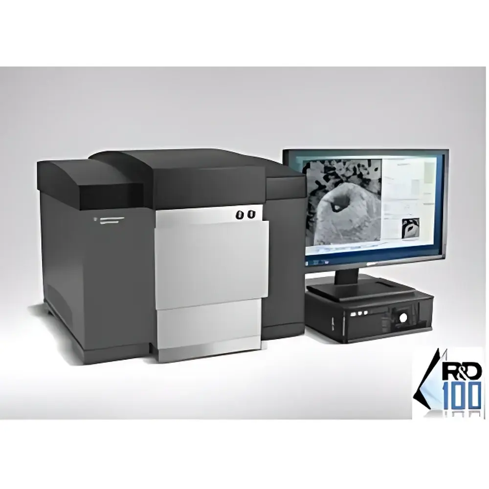
Agilent 8500FE Desktop Field-Emission Scanning Electron Microscope
| Origin | USA |
|---|---|
| Manufacturer Type | Authorized Distributor |
| Origin Category | Imported |
| Model | 8500 |
| Price Range | USD 135,000 – 205,000 (FOB) |
| Electron Gun Type | Cold Field-Emission (CFE) |
| Secondary Electron Imaging Resolution | 10 nm @ 1 kV |
| Magnification Range | 250× – 800,000× |
| Accelerating Voltage | 0.5 – 2.0 kV |
Overview
The Agilent 8500FE is a compact, high-performance desktop field-emission scanning electron microscope engineered for precision low-voltage imaging in space-constrained laboratory environments. Unlike conventional thermionic or Schottky-emission SEMs, the 8500FE employs a cold field-emission (CFE) electron source, delivering exceptional brightness and spatial coherence at accelerating voltages as low as 0.5 kV. This enables high-contrast surface imaging of beam-sensitive, non-conductive, or uncoated specimens—without requiring carbon or gold sputter coating—by minimizing charging artifacts and maximizing secondary electron yield. Its optimized electrostatic lens column eliminates magnetic hysteresis and drift, ensuring stable probe positioning and long-term reproducibility across repeated imaging sessions. Designed for integration into standard benchtop workflows, the system operates without external cooling water, active vibration isolation platforms, or dedicated electrical infrastructure—only a standard grounded 120/230 VAC outlet is required.
Key Features
- Cold field-emission electron gun with ultra-high brightness and sub-nanometer energy spread, enabling superior signal-to-noise ratio at low kV
- Electrostatic condenser and objective lens architecture—free from magnetic remanence—ensuring repeatable alignment and eliminating need for routine stigmator recalibration
- Integrated motorized XYZ sample stage with programmable positioning, step resolution ≤ 0.1 µm, and coordinate memory for multi-site acquisition
- Optimized low-kV imaging optics delivering 10 nm secondary electron resolution at 1 kV—performance comparable to full-size CFE-SEM systems
- Compact footprint (≤ 0.8 m² floor space) and self-shielded vacuum chamber compatible with ambient lab environments (no Faraday cage required)
- Automated vacuum interlock and pressure monitoring compliant with IEC 61000-6-4 electromagnetic compatibility standards
Sample Compatibility & Compliance
The 8500FE supports direct imaging of insulating materials—including polymers, ceramics, biological tissues, and geological samples—without conductive coating, thanks to its stable low-voltage operation and charge compensation capability. Specimen dimensions up to Ø 50 mm × 25 mm height are accommodated using standard stub mounts. The system meets ISO 14644-1 Class 8 cleanroom requirements for internal chamber particulate control and complies with ASTM E1558–22 for SEM resolution verification procedures. All operational parameters—including kV, working distance, dwell time, and detector bias—are logged with timestamped metadata to support GLP/GMP audit trails per FDA 21 CFR Part 11 guidelines when paired with validated software configurations.
Software & Data Management
Acquisition and analysis are managed via Agilent SEM Control Suite v3.2—a Windows-based application supporting real-time image streaming, batch acquisition scripting, and automated focus/stigmation routines. Raw data is stored in open-format TIFF with embedded EXIF metadata (including kV, WD, magnification, detector gain, and stage coordinates). Export options include CSV for quantitative morphology metrics (particle size distribution, aspect ratio, Feret diameter), and standardized HDF5 containers for interoperability with third-party image analysis platforms (e.g., ImageJ/Fiji, MATLAB, Python scikit-image). Audit logs record user ID, session start/end timestamps, parameter modifications, and export events—configurable for electronic signature validation.
Applications
- Materials science: Nanoscale characterization of battery electrode coatings, thin-film delamination, and catalyst particle dispersion
- Life sciences: High-fidelity imaging of freeze-dried cells, pollen surfaces, and uncoated tissue sections at native hydration states
- Quality control: Rapid failure analysis of microelectronics packaging, solder joint integrity, and MEMS device topography
- Geosciences: Mineral phase identification and pore-network analysis in shale and carbonate rock fragments
- Forensics: Fiber morphology comparison, gunshot residue particle morphology, and trace evidence surface topography
FAQ
Does the 8500FE require liquid nitrogen or external cooling?
No—the cold field-emission source is maintained at room temperature via ultra-high vacuum (<1×10⁻⁸ Torr) and does not rely on cryogenic cooling.
Can it image hydrated biological samples?
The 8500FE operates under high vacuum; therefore, fully hydrated specimens require prior critical-point drying or freeze-drying. Environmental SEM modes are not supported.
What maintenance intervals are recommended?
Annual vacuum system inspection and filament performance validation are advised. The CFE tip typically exceeds 12 months of continuous operation under standard usage conditions.
Is remote operation supported?
Yes—via secure RDP or VNC over local network; firewall-configured TLS-encrypted web interface optional for off-site diagnostics.
How is resolution verified per international standards?
Using certified NIST-traceable resolution test gratings (e.g., SPI #2721A), following ASTM E1558–22 line-pair measurement methodology with ≥5 independent measurements per condition.


