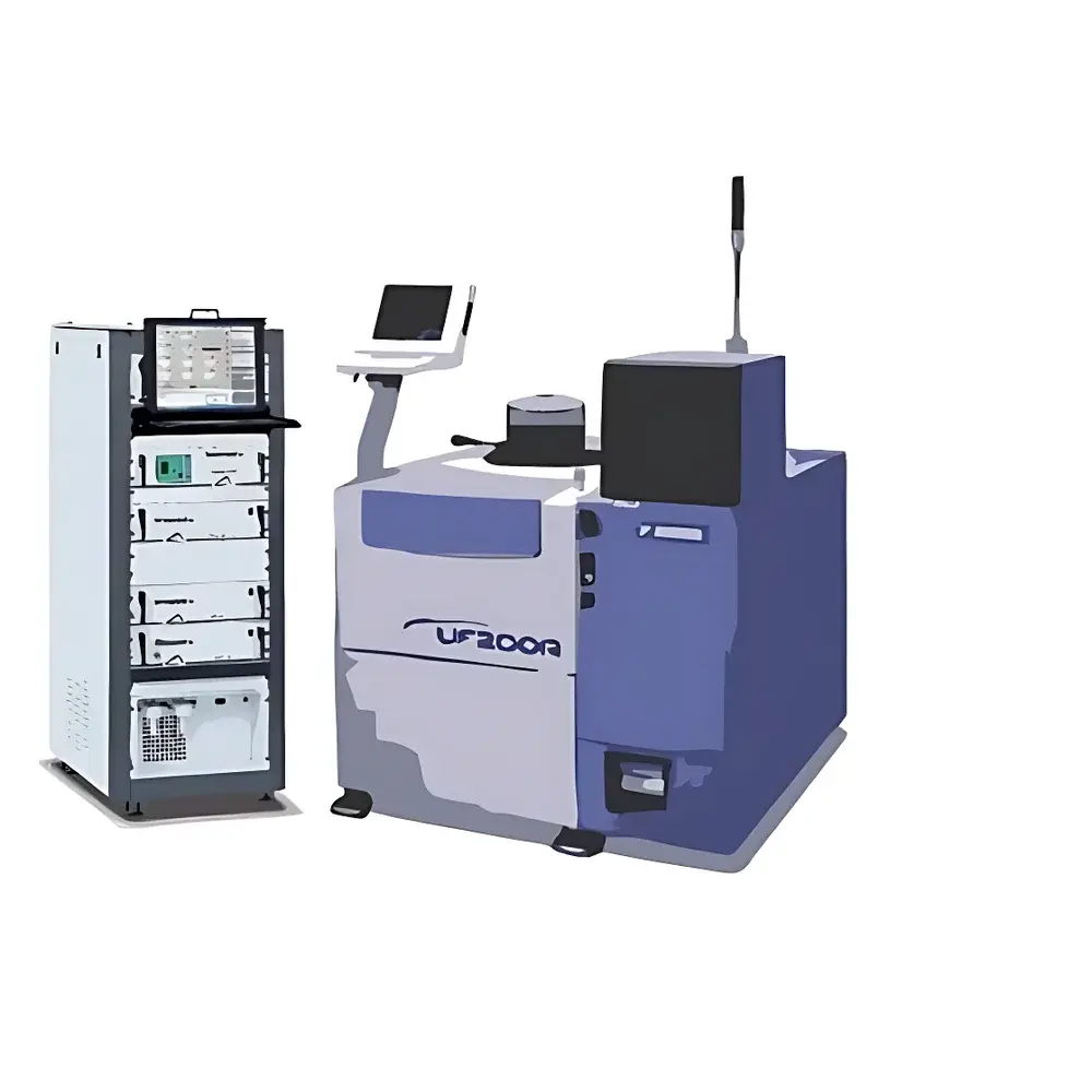
Hprobe Speed-Up Wafer-level Magnetic Test System
| Origin | USA |
|---|---|
| Manufacturer Type | Authorized Distributor |
| Origin Category | Imported |
| Model | Speed-Up Wafer-level Magnetic Test |
| Price | Upon Request |
Overview
The Hprobe Speed-Up Wafer-level Magnetic Test System is a precision-engineered platform for magnetic characterization and functional testing of semiconductor devices at the wafer level—designed specifically for R&D, process development, and high-reliability qualification of magnetic thin-film devices. It operates on the principle of controlled 3D vector magnetic field application synchronized with high-fidelity electrical stimulus and measurement, enabling full electro-magnetic co-characterization under programmable field conditions. Unlike conventional probe stations limited to DC bias or rudimentary field exposure, this system integrates a patented triaxial magnetic field generator directly above the chuck—delivering localized, dynamically tunable fields (up to ±2 T) with sub-degree angular resolution and nanosecond-scale temporal control. Its architecture conforms to SEMI-compliant wafer handling standards and supports seamless integration into automated test environments for MRAM (STT, SOT, VCMA), spintronic sensors (AMR, GMR, TMR), and magnetic MEMS.
Key Features
- Triaxial magnetic field generation with independent X/Y/Z axis control, enabling arbitrary static field orientation and continuous rotational field synthesis
- Integrated 3D Hall sensor calibration system with ±0.1° angular accuracy, 5 V/T sensitivity, ±2 T range, differential output, and <100 ppm/°C thermal drift compensation
- Z-axis gap between field generator and wafer adjustable from 500 µm to 5 mm (standard 1 mm), optimized for field homogeneity and probe access
- Full-wafer compatibility: supports 100 mm (manual), 200 mm, and 300 mm (fully automated) platforms with thermal chucks (–60 °C to +150 °C), integrated wafer alignment optics, and broken-wafer handling options
- Modular instrumentation suite including source measure units (SMUs), 18-bit DMMs, 40 MHz dual-channel AWGs, and sub-300 ps pulse generators—all synchronized via deterministic low-jitter triggers (<35 ps RMS)
- Field-synchronized measurement capability: simultaneous acquisition of I-V, R-V, pulse write/read, tunnel magnetoresistance (TMR), bit-error rate (BER), and (I,V,H) parametric mapping
Sample Compatibility & Compliance
The system accommodates standard probe cards and custom micro-manipulated DC/RF probes, subject only to the mechanical constraint that the field generator–wafer gap remains ≤1 mm during high-field operation to preserve field fidelity. It complies with SEMI E10 (Specification for Definition and Measurement of Equipment Reliability and Availability), SEMI E19 (Wafer Map Data Standard), and supports audit-ready data traceability per FDA 21 CFR Part 11 and ISO/IEC 17025 requirements when configured with electronic signatures and secure user-role management. All magnetic calibrations are traceable to NIST-certified reference standards via embedded Hall sensor validation protocols.
Software & Data Management
The unified test software operates in three configurable modes: Calibration (for field configuration and user-defined pattern definition), Engineering (for scripted parametric sweeps, custom algorithm implementation, and real-time visualization), and Production (for optimized throughput with recipe-based execution and statistical process control export). The environment supports Python API integration for advanced automation, HDF5-based binary data storage with metadata tagging (field vector, temperature, timestamp, instrument settings), and direct export to JMP, MATLAB, or SPICE-compatible formats. Audit trails record all parameter changes, calibration events, and user actions with immutable timestamps—ensuring GLP/GMP compliance in regulated development workflows.
Applications
- STT-MRAM and SOT-MRAM switching threshold mapping under rotating and pulsed field conditions
- Voltage-controlled magnetic anisotropy (VCMA) coefficient extraction via concurrent electric field and magnetic field sweep
- TMR sensor linearity, hysteresis, and offset characterization across field orientation space
- Spin-orbit torque efficiency quantification in heavy-metal/ferromagnet heterostructures
- Dynamic magnetization reversal dynamics via time-resolved pulse testing (sub-ns resolution)
- Process variation analysis across die and wafer using spatially resolved (I,V,H) phase diagrams
FAQ
What wafer sizes does the Hprobe Speed-Up system support?
It supports 100 mm (manual prober), 200 mm, and 300 mm (fully automated) wafers—with compatible chucks, aligners, and load mechanisms meeting SEMI F47 specifications.
Is the magnetic field generator compatible with RF probing?
Yes—provided the probe pitch and geometry maintain ≥1 mm clearance between the field generator and wafer surface; RF probes must be non-magnetic and rated for operation within ±2 T static fields.
How is field calibration performed and maintained?
Calibration uses the integrated 3D Hall sensor array mounted on the chuck. Users perform in situ field mapping at user-defined points, generating correction matrices applied in real time during test execution—no external calibration fixtures required.
Can the system perform time-resolved measurements under magnetic field modulation?
Yes—via hardware synchronization between the AWG/pulse generator and SMU/DMM, enabling triggered acquisition windows as short as 1 µs with field ramp rates up to 10⁶ T/s.
Does the software support custom algorithm development for magnetic parameter extraction?
Yes—the Engineering mode provides full Python scripting access to instrument drivers, field control APIs, and raw data buffers, enabling implementation of custom fitting routines (e.g., Stoner-Wohlfarth modeling, Néel-Brown relaxation analysis).


")