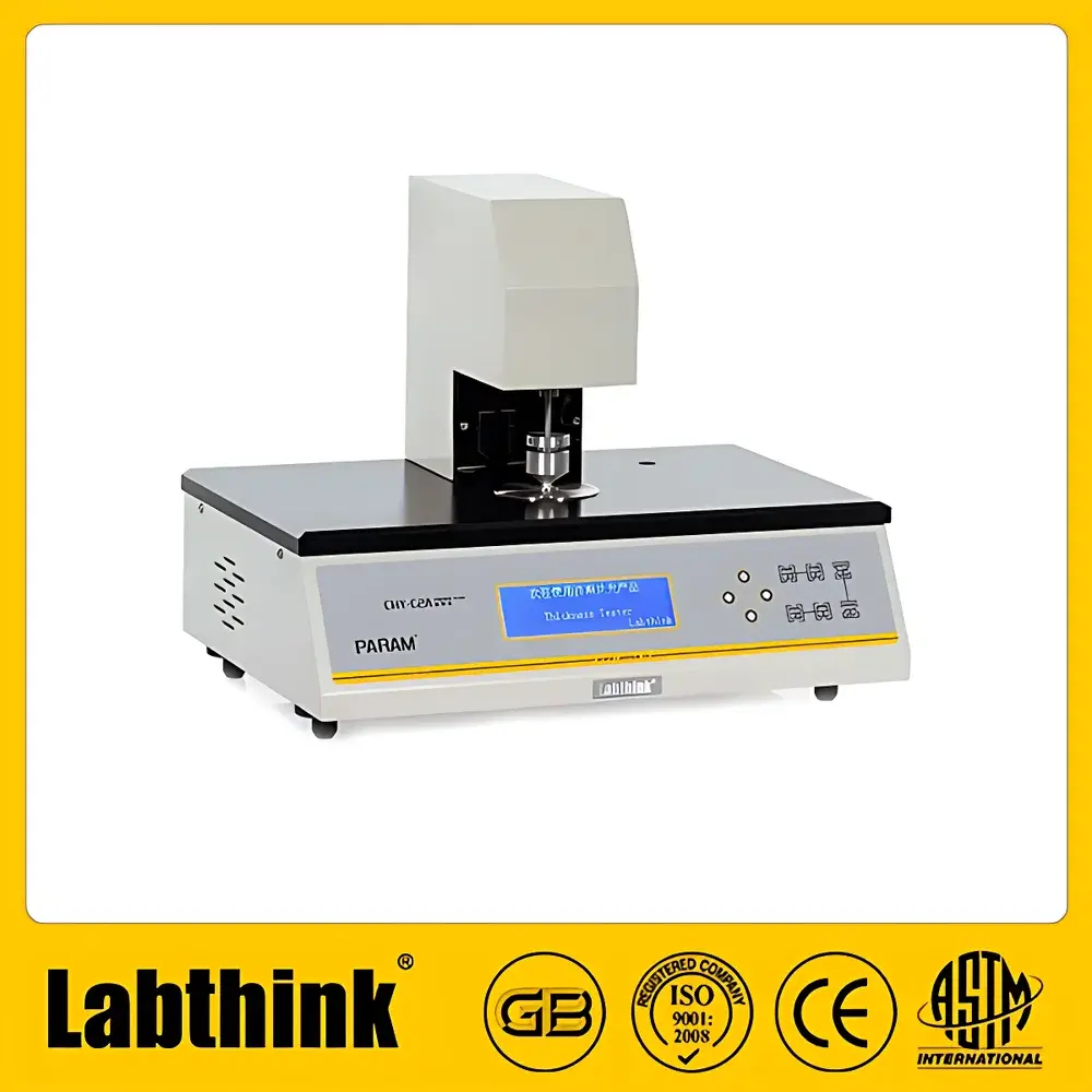
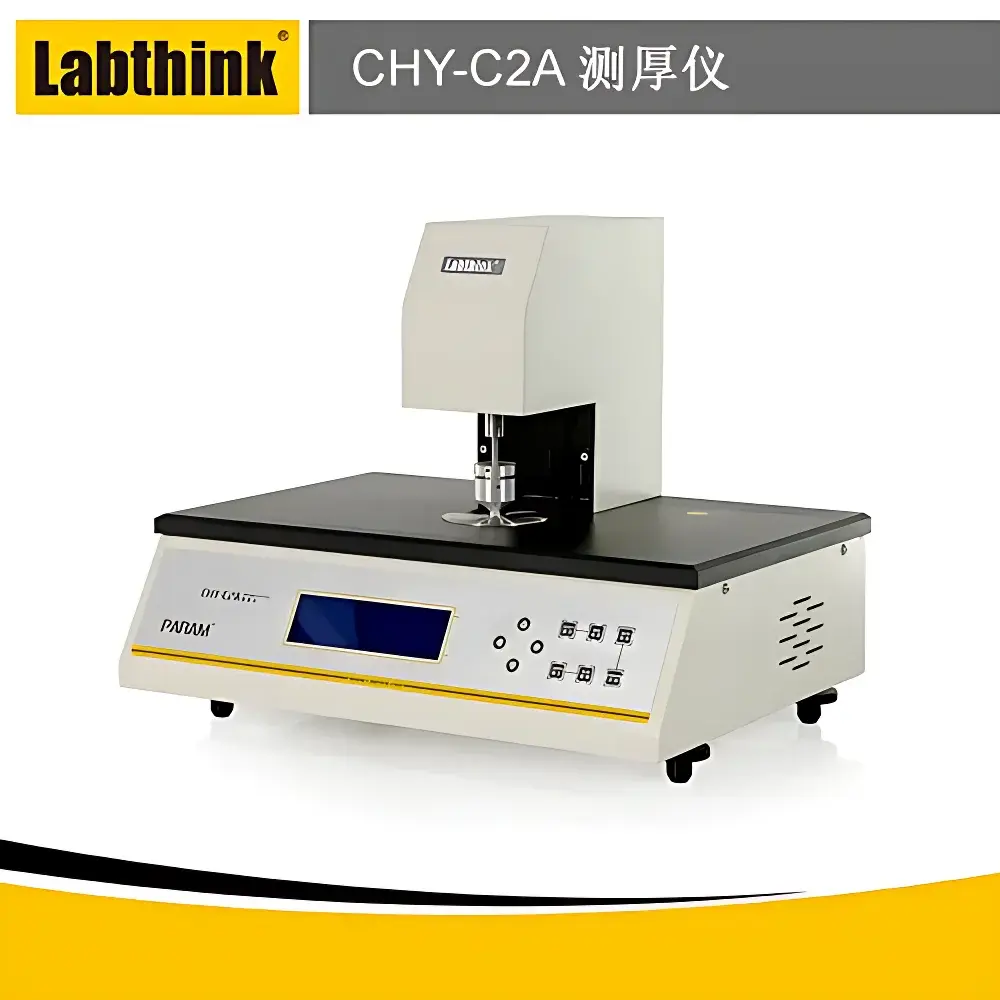
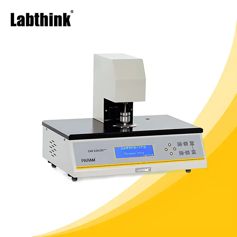
Labthink CHY-C2A Mechanical Contact Thickness Gauge for Silicon Wafers and Thin Films
| Brand | Labthink |
|---|---|
| Model | CHY-C2A |
| Measurement Principle | Mechanical Contact (ISO/ASTM-Compliant) |
| Load Range | 0–2 mm (standard), up to 12 mm (optional) |
| Resolution | 0.1 µm |
| Measuring Speed | 10 tests/min (adjustable) |
| Contact Area | 50 mm² (films), 200 mm² (paper) |
| Measurement Pressure | 17.5 ± 1 kPa (films), 50 ± 1 kPa (paper) |
| Compliance | ISO 4593, ISO 534, ISO 3034, GB/T 6672, GB/T 451.3, ASTM D374, ASTM D1777, TAPPI T411, JIS K6250, JIS K6783, JIS Z1702, BS 3983, BS 4817 |
| Interface | RS232 |
| Data Management | Lystem™ Lab Data Sharing System |
| Power Supply | 220 VAC 50 Hz / 120 VAC 60 Hz |
| Dimensions | 461 × 334 × 357 mm (L×W×H) |
| Net Weight | 32 kg |
Overview
The Labthink CHY-C2A Mechanical Contact Thickness Gauge is a precision metrology instrument engineered for high-reproducibility thickness measurement of rigid and semi-rigid planar materials—particularly silicon wafers used in photovoltaic cell manufacturing, as well as polymer films, battery separator membranes, metallic foils, paperboard, and technical papers. It operates on the fundamental principle of controlled mechanical contact: a calibrated, pneumatically or gravity-assisted measuring head applies standardized pressure to the sample surface while a high-resolution linear variable differential transformer (LVDT) sensor records displacement with sub-micron resolution. This method ensures traceability to international standards and eliminates optical interference issues common in non-contact techniques (e.g., laser triangulation or interferometry), making it especially suitable for matte, translucent, or highly reflective surfaces such as polished silicon substrates. Designed for laboratory and QC environments in semiconductor fabrication, battery R&D, packaging development, and papermaking industries, the CHY-C2A delivers stable, operator-independent results under GLP-compliant workflows.
Key Features
- Standardized mechanical contact geometry: dual-contact-area configuration (50 mm² for thin films; 200 mm² for thicker substrates) with precisely regulated measurement pressures (17.5 ± 1 kPa for films; 50 ± 1 kPa for paper)—fully compliant with ISO 4593 and ASTM D374 requirements.
- Motorized auto-lift measuring head: eliminates manual handling errors and ensures consistent approach velocity and dwell time, critical for minimizing elastic recovery effects in viscoelastic materials.
- Dual operation modes: fully automated batch testing (programmable test count, interval, and statistical output) and manual single-point measurement for rapid verification or troubleshooting.
- Real-time statistical analysis: on-screen display of max/min/mean values, standard deviation (σ), coefficient of variation (CV%), and histogram distribution per test set—enabling immediate assessment of material uniformity.
- Integrated calibration traceability: includes NIST-traceable stainless-steel reference gauge blocks (certified to ±0.2 µm uncertainty) for daily system verification and periodic recalibration.
- Modular hardware architecture: supports optional accessories including extended-range measuring heads (up to 12 mm stroke), programmable pneumatic loading modules, thermal-controlled sample stages (-10 °C to +60 °C), and direct thermal printer integration.
Sample Compatibility & Compliance
The CHY-C2A accommodates flat, non-porous specimens with dimensions ≥ 50 mm × 50 mm and surface flatness ≤ 10 µm PV. Verified compatibility includes monocrystalline and multicrystalline silicon wafers (125–210 mm diameter, 160–180 µm typical thickness), lithium-ion battery anode/cathode coatings on Cu/Al foil, polyethylene and polypropylene microporous separators, PET and BOPP packaging films, and corrugated board liners. All measurement protocols adhere to ISO/IEC 17025 principles for testing laboratories. The instrument’s pressure and area specifications are explicitly validated against ISO 534 (paper and board), ISO 4593 (plastic film), and ASTM D1777 (textile thickness), ensuring data acceptance in regulatory submissions—including FDA-reviewed battery safety dossiers and IEC 61215-certified PV module qualification reports.
Software & Data Management
The CHY-C2A interfaces seamlessly with Labthink’s Lystem™ Laboratory Data Sharing System—a secure, audit-ready platform supporting 21 CFR Part 11 compliance. Lystem™ provides electronic signature capability, role-based user access control, immutable audit trails for all measurement events (including calibration logs, parameter changes, and result exports), and automated report generation in PDF/A-1b or CSV formats. Raw data export via RS232 enables integration with enterprise LIMS (e.g., Thermo Fisher SampleManager, LabVantage) and statistical process control (SPC) tools like Minitab or JMP. Optional PC-based software adds advanced features: multi-instrument synchronization, SPC charting (X̄-R, Cpk), Gage R&R study support, and custom test method scripting for complex multi-step protocols.
Applications
- Photovoltaic manufacturing: routine thickness verification of silicon wafers pre- and post-texturing, anti-reflective coating deposition, and metallization—ensuring wafer bow and thickness variation remain within ±2 µm tolerance bands required for high-efficiency cell yield.
- Lithium-ion battery development: quantitative assessment of electrode calendering uniformity, separator dimensional stability under compression, and dry-film thickness consistency across pilot-coating lines.
- Packaging R&D: validation of barrier film lamination integrity, thickness distribution mapping of coextruded structures, and correlation of gauge banding with extrusion die settings.
- Quality assurance in paper mills: determination of basis weight equivalence through thickness-density relationships per TAPPI T411, and detection of caliper variation affecting print registration accuracy.
- Academic materials science: in-situ thickness monitoring during solvent-cast film drying, thermal expansion coefficient derivation, and creep behavior analysis under sustained load.
FAQ
What is the minimum measurable thickness for silicon wafers using the CHY-C2A?
The instrument achieves reliable repeatability down to 50 µm for rigid, polished silicon substrates when using the 50 mm² contact foot and 17.5 kPa load. Below this, surface roughness and edge effects dominate measurement uncertainty.
Can the CHY-C2A measure curved or flexible samples?
No—it is strictly designed for flat, dimensionally stable specimens. Curved or highly compliant materials (e.g., hydrogels, soft elastomers) require non-contact profilometry or capacitance-based gauges.
Is firmware upgrade supported remotely?
Yes—Labthink provides quarterly firmware updates via encrypted USB key or authenticated Lystem™ cloud sync, including enhanced statistical algorithms and expanded standard library support.
How often must the system be calibrated?
Daily verification with supplied gauge blocks is mandatory before first use; full calibration by an accredited metrology lab is recommended every 12 months—or after any impact event or mechanical maintenance.
Does the CHY-C2A meet requirements for ISO 9001 internal audits?
Yes—the built-in calibration traceability, full audit trail in Lystem™, and documented uncertainty budgets satisfy Clause 7.1.5.2 (Monitoring and measuring resources) and Annex A.1 (Measurement traceability) of ISO 9001:2015.
")


