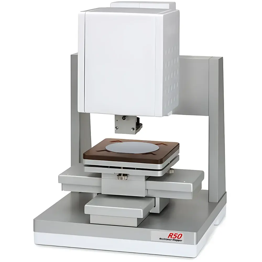
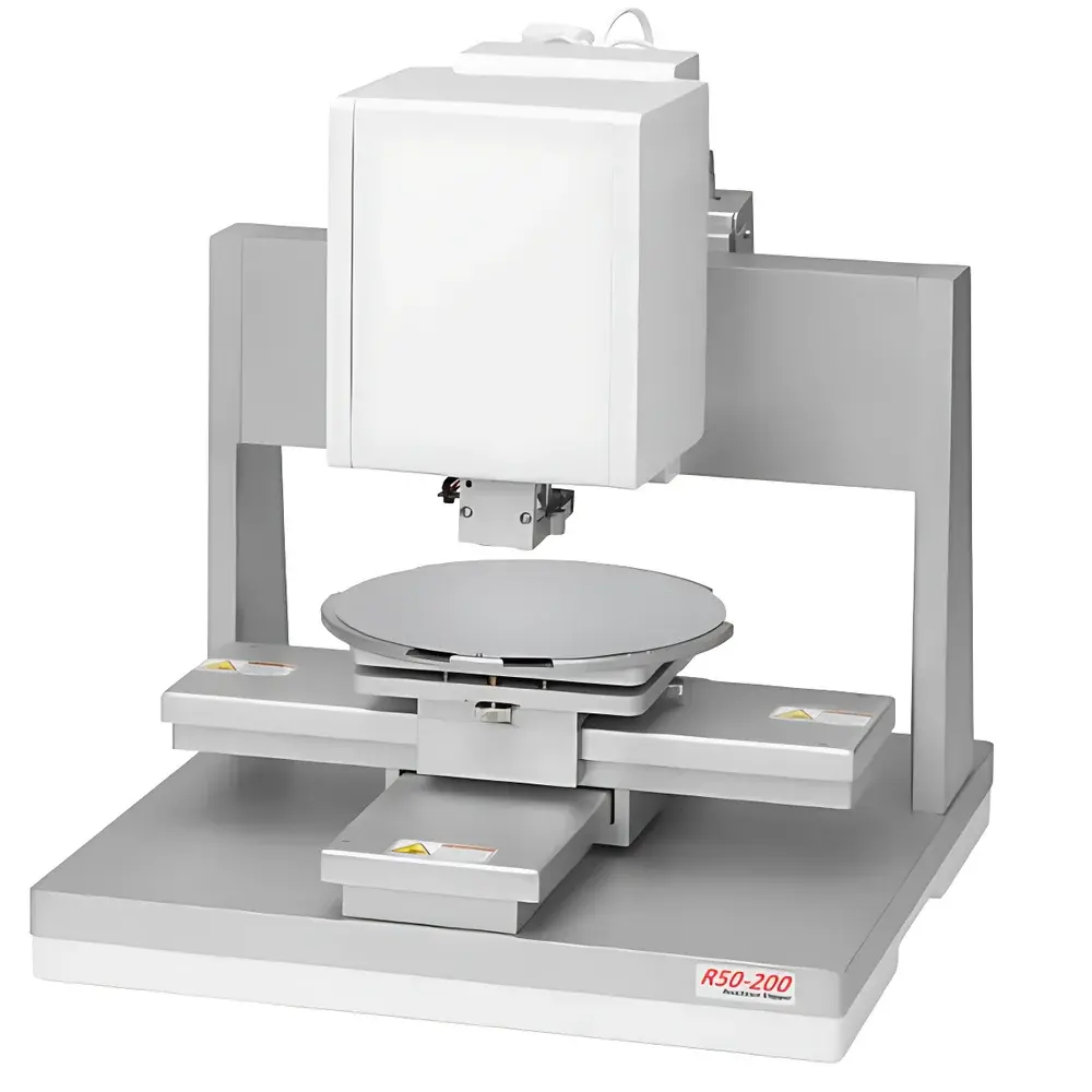
KLA R50-4PP / R50-EC Four-Point Probe & Eddy Current Resistivity Mapping System
| Brand | KLA |
|---|---|
| Origin | Malaysia |
| Model | R50-4PP / R50-EC |
| Type | Imported Instrument |
| Distribution Channel | Authorized Distributor |
| Pricing | Available Upon Request |
Overview
The KLA R50-4PP and R50-EC are precision-engineered, dual-mode thin-film electrical characterization systems designed for high-reproducibility mapping of sheet resistance (Rs), resistivity (ρ), conductivity (σ), and metallic layer thickness. The R50-4PP implements a guarded four-point probe (4PP) technique based on the van der Pauw and linear array methodologies—ensuring accurate, contact-based DC resistivity measurement with minimal current injection artifacts. In contrast, the R50-EC employs high-frequency eddy current induction (typically 1–10 MHz) to non-invasively quantify conductive film thickness and sheet resistance on delicate, flexible, or passivated substrates where physical contact is undesirable or mechanically prohibitive. Both configurations share a common modular platform featuring motorized Z-axis travel (>25 mm), programmable X-Y stage positioning, and sub-micron repeatability—enabling robust metrology across wafer-scale samples up to 200 mm diameter.
Key Features
- Modular dual-mode architecture: Selectable four-point probe (R50-4PP) or eddy current (R50-EC) head—field-upgradable without hardware replacement
- Wide dynamic range: Sheet resistance measurement from 0.1 mΩ/□ to 10 MΩ/□ (10 orders of magnitude), supporting ultra-thin metal films (<1 nm) and heavily doped semiconductors
- Automated Z-axis compensation: Real-time probe force control (0.5–5 g) and vertical travel >25 mm ensure consistent contact pressure and step-height tolerance on patterned wafers
- High-resolution mapping: 1 µm positional repeatability over 200 mm × 200 mm travel range; supports grid, spiral, and user-defined scan patterns
- Integrated environmental shielding: Optional light-tight enclosure (standard on R54 series) eliminates photoconductive interference during ion-implanted or epitaxial wafer characterization
- Thermal drift compensation: Onboard temperature sensor and algorithmic correction maintain <±0.3% Rs stability over 8-hour continuous operation
Sample Compatibility & Compliance
The R50 platform accommodates rigid and flexible substrates including silicon wafers (100–300 mm), glass, sapphire, polyimide, PET, and ceramic carriers. It supports both flat and slightly warped samples (up to 50 µm bow) via active Z-height tracking. All measurement protocols comply with ASTM F84-22 (Standard Test Method for Sheet Resistance of Semiconductor Wafers Using a Collinear Four-Point Probe), ISO 10474 (Metallic coatings — Measurement of sheet resistance), and SEMI MF1530 (Guide for Electrical Characterization of Conductive Thin Films). Data acquisition meets GLP/GMP documentation requirements, with optional 21 CFR Part 11-compliant audit trail and electronic signature modules available for regulated semiconductor fabrication environments.
Software & Data Management
KLA’s Filmetrics Metrology Suite v5.x provides full instrument control, real-time contour mapping, statistical process control (SPC) charting, and cross-platform data export (CSV, HDF5, .mat). The software includes built-in calibration wizards for probe spacing verification, eddy current frequency tuning, and substrate permittivity compensation. Raw voltage/current traces, impedance spectra, and spatial metadata are stored with timestamped headers and operator ID. Exported datasets retain traceability to NIST-traceable reference standards (e.g., NIST SRM 2136). Batch reporting supports custom templates aligned with internal quality management systems (QMS) and automated PDF generation with embedded measurement uncertainty budgets.
Applications
- Semiconductor process development: Ion implant dose verification, epitaxial layer uniformity assessment, and anneal optimization via Rs mapping
- Compound semiconductor manufacturing: GaN-on-Si, SiC, and InP wafer-level qualification for power electronics and RF devices
- Flexible electronics: Thickness and continuity validation of ITO, Ag nanowire, graphene, and PEDOT:PSS layers on roll-to-roll substrates
- Photovoltaics: Transparent conductive oxide (TCO) homogeneity analysis on CIGS and perovskite solar cells
- Advanced packaging: Cu redistribution layer (RDL) integrity screening and bump under-bump metallization (UBM) thickness correlation
- Academic research: Correlation of carrier concentration, mobility, and scattering mechanisms in 2D materials using multi-frequency eddy current spectroscopy
FAQ
What is the difference between four-point probe and eddy current measurement modes?
Four-point probe provides absolute DC sheet resistance values with sub-1% uncertainty on planar, conductive surfaces but requires physical contact. Eddy current offers non-contact, high-speed mapping ideal for fragile, coated, or temperature-sensitive films—though it requires empirical or physics-based calibration for quantitative thickness extraction.
Can the R50 system measure through dielectric layers?
Yes—the R50-EC configuration can penetrate insulating layers up to ~1 µm thick (e.g., SiO₂, SiNx, photoresist) depending on frequency selection and substrate conductivity. The R50-4PP requires direct metal exposure.
Is the system compatible with cleanroom Class 100 environments?
All R50 variants are rated for ISO Class 5 (Class 100) operation; optional stainless-steel housing and static-dissipative components are available upon request.
How is probe alignment verified and maintained?
Each 4PP head includes an integrated optical alignment camera and auto-focus routine. Tip wear is monitored via periodic contact resistance trending and tip geometry inspection using the included USB microscope accessory kit.
Does the system support automated recipe-based measurements for production line integration?
Yes—Filmetrics Metrology Suite supports SECS/GEM protocol compliance and PLC-triggered measurement sequences via digital I/O interface, enabling seamless integration into factory automation systems.


