X-RAY Automated Semiconductor Die & Wire Bond Inspection System
| Brand | Zhengye |
|---|---|
| Model | Zhengye X-RAY AutoInspection System |
| Origin | Guangdong, China |
| Manufacturer Type | OEM/ODM Manufacturer |
| Regional Classification | Domestic (China) |
| Price Range | USD 112,000 – 140,000 |
Overview
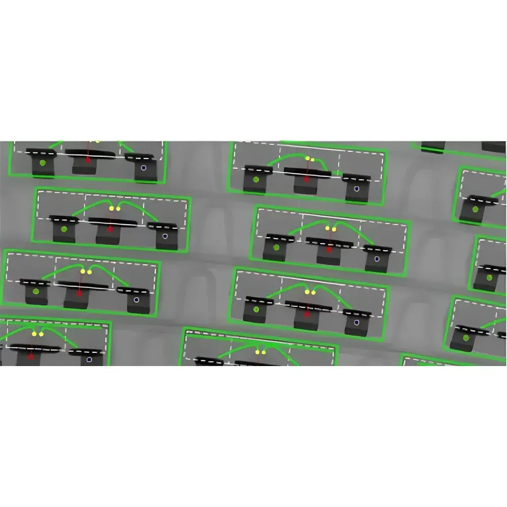
The Zhengye X-RAY AutoInspection System is an industrial-grade, fully automated non-destructive testing (NDT) platform engineered for high-throughput, high-fidelity internal inspection of semiconductor packages—specifically targeting wire-bonded die assemblies in QFN, BGA, SOP, and similar leadframe- or substrate-based packages. Utilizing microfocus X-ray imaging (typically 90–130 kV source voltage, <5 µm focal spot size), the system captures high-contrast transmission radiographs to resolve sub-micron structural features including bond wires (25–500 µm diameter), die attach voids, mold compound delamination, and interfacial anomalies. Unlike manual or semi-automated X-ray stations, this system integrates real-time image acquisition, multi-angle tomographic reconstruction (optional), and AI-accelerated defect classification within a single workflow—designed to meet the repeatability, traceability, and throughput requirements of front-end packaging lines and post-assembly QA labs.
Key Features
- Fully motorized XYZθ stage with ±0.5 µm positioning repeatability and programmable tilt (±90°) for oblique-angle wire bond visualization
- High-resolution flat-panel detector (≥ 3072 × 3072 pixels, 75 µm pixel pitch) coupled with tungsten-target microfocus X-ray source (≤ 3 W power, <5 µm focal spot)
- Real-time image enhancement pipeline: dynamic range compression, noise suppression (non-local means filtering), and edge-aware contrast optimization
- Embedded GPU-accelerated inference engine supporting on-device deployment of convolutional neural networks trained on >200,000 annotated wire bond images
- Integrated pass/fail decision logic per IPC-A-610 and JEDEC J-STD-006 criteria, with configurable sensitivity thresholds for void area %, wire sweep angle, neck height deviation, and ball bond geometry
- Modular software architecture compliant with SEMI E10 (Definition of Equipment Reliability and Maintainability) and ISO 9001:2015 documentation standards
Sample Compatibility & Compliance
The system accommodates standard JEDEC trays (TR, TA, TE), gel packs, and bare PCBs up to 300 × 300 mm. It supports automatic tray indexing and fiducial-based alignment for batch inspection of up to 128 units per cycle. All measurement protocols adhere to ASTM E2698-21 (Standard Practice for Radioscopic Examination of Electronic Components) and align with failure analysis workflows defined in JESD22-A102 (Temperature Cycling) and JESD22-A108 (Bias-Humidity Testing). Full audit trail logging—including operator ID, timestamp, exposure parameters, ROI coordinates, and classification confidence scores—is retained for GLP/GMP compliance and FDA 21 CFR Part 11 readiness (electronic signature support available via optional module).
Software & Data Management
Zhengye VisionInsight™ v4.2 provides unified control of hardware, image processing, and reporting. The software includes: (i) customizable recipe management with version-controlled inspection templates; (ii) hierarchical defect taxonomy mapping to industry-standard failure modes (e.g., “wire lift-off”, “ball bond voiding”, “neck cracking”); (iii) statistical process control (SPC) dashboard with Cpk/Ppk calculation, trend analysis, and OCAP (Out-of-Control Action Plan) triggers; (iv) export capability to CSV, XML, and PDF formats with embedded radiograph thumbnails and measurement overlays; (v) RESTful API interface for integration with MES (e.g., Siemens Opcenter, Camstar) and factory-wide data lakes.
Applications
- Automated final test verification of wire bond integrity prior to burn-in or shipment
- Root cause analysis of early-life failures in automotive-grade ICs (AEC-Q100 Grade 1/2)
- In-line monitoring of thermosonic bonding process stability across multiple shift operations
- Qualification of new package designs (e.g., stacked-die FCBGA, fan-out wafer-level packages)
- Supporting FA labs in correlating X-ray findings with cross-section SEM/EDS results
- Supplier qualification audits requiring objective, operator-independent defect scoring
FAQ
Does the system support both 2D radiography and computed laminography (CL)?
Yes—standard configuration includes dual-axis (X/Y) radiography; optional CL module enables depth-resolved slicing of bond wires in high-I/O packages.
What training and validation documentation is provided?
Each unit ships with IQ/OQ/PQ protocols, Gage R&R study templates, and a certified reference set of NIST-traceable phantom samples (wire bond geometry standards, void size gradation chips).
Can defect classification models be retrained on customer-specific failure modes?
Yes—VisionInsight™ supports secure model import/export and includes a labeled dataset ingestion toolkit compatible with common annotation formats (COCO, Pascal VOC).
Is remote diagnostics and firmware update supported?
Yes—via TLS-secured HTTPS channel with configurable firewall rules; all updates undergo SHA-256 signature verification and rollback capability.
What is the typical throughput for a 16-pin SOIC package?
Approximately 4.2 seconds per unit at 10 µm resolution, including auto-alignment, dual-angle imaging, and AI classification—scalable to >8,500 units/shift in continuous operation mode.


