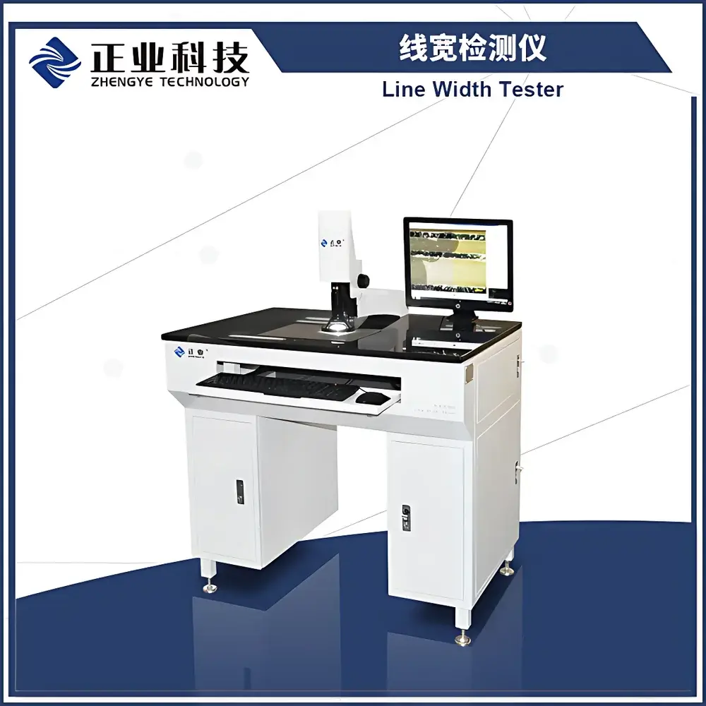
Zhengye PCB Line Width Inspection System DV-PCB200
| Brand | Zhengye |
|---|---|
| Origin | Guangdong, China |
| Manufacturer Type | OEM/ODM Manufacturer |
| Country of Origin | China |
| Model | DV-PCB200 |
| Pricing | Available Upon Request |
Overview
The Zhengye PCB Line Width Inspection System DV-PCB200 is a high-precision optical metrology platform engineered for non-contact, real-time dimensional verification of printed circuit board (PCB) features during mid- to late-stage fabrication. It operates on the principle of digital image-based edge detection using high-resolution monochrome CMOS imaging coupled with calibrated telecentric optics and stable red LED illumination. Designed for inline or benchtop deployment in PCB manufacturing cleanrooms, the system delivers traceable measurements of conductor geometry—including upper and lower line widths (after etching, pre-solder mask), line-to-line spacing, pad-to-trace clearance, drill-to-copper distance, and critical feature diameters such as through-holes, blind vias, and curved contours. Its measurement architecture supports ISO 17025-aligned calibration protocols and is routinely validated against NIST-traceable step-height and linewidth standards.
Key Features
- Precision Optical Metrology: Equipped with motorized precision focus adjustment and telecentric lens assembly to minimize perspective error; achieves sub-pixel edge localization via centroid-based sub-pixel interpolation algorithms.
- Automated Edge Detection Engine: Implements adaptive thresholding, morphological noise suppression, and multi-scale gradient analysis to robustly identify copper trace boundaries—even on partially oxidized or micro-roughened surfaces.
- Red LED Targeting Illumination: Integrated coaxial red LED ring light ensures consistent, glare-free contrast enhancement across varied surface finishes (e.g., bare copper, HASL, ENIG), reducing operator dependency and improving repeatability.
- Real-Time SPC Integration: Built-in statistical process control module computes Cp/Cpk, X-bar & R charts, histogram distributions, and trend analysis directly from measurement datasets—exportable in CSV or XML format for MES integration.
- Modular Software Architecture: Supports dual-mode operation: manual point-and-measure for R&D validation, and batch-programmed auto-run mode for production lot sampling per IPC-6012 or IPC-A-600 inspection criteria.
Sample Compatibility & Compliance
The DV-PCB200 accommodates rigid, flex, and rigid-flex PCB substrates up to 610 mm × 460 mm (24″ × 18″) and thicknesses ranging from 0.05 mm to 3.2 mm. It is validated for use on IC substrates (e.g., ABF film, silicon interposers), thin-film transistor (TFT) arrays, and LCD photomasks with line widths ≥ 5 µm and pitch ≥ 10 µm. Measurement procedures conform to IPC-TM-650 Section 2.2.15 (Optical Microscopy for Dimensional Verification) and support audit readiness for ISO 9001, IATF 16949, and IPC Class 3 manufacturing environments. Optional GLP-compliant audit trail logging meets FDA 21 CFR Part 11 requirements when paired with validated software version 3.2+.
Software & Data Management
Zhengye VisionSuite™ v4.1 (included) provides intuitive GUI-driven measurement workflows, customizable inspection templates, and hierarchical data organization by job ID, panel ID, and layer designation. All measurement records are timestamped, user-ID stamped, and stored with full metadata—including camera exposure time, lens magnification, focus position, and environmental temperature/humidity tags (when connected to optional sensor hub). Raw images and annotated overlays are archived in lossless TIFF format; statistical summaries comply with MSA (Measurement Systems Analysis) guidelines per AIAG MSA 4th Edition. Data export supports direct OPC UA handshake with factory SCADA systems and seamless import into JMP, Minitab, or custom Python-based analytics pipelines.
Applications
- Post-etch line width uniformity assessment on inner/outer layers prior to solder mask application
- Verification of fine-pitch routing compliance in HDI and mSAP processes
- Dimensional release testing for automotive-grade PCBs (AEC-Q200 qualified designs)
- Process capability studies during DOE (Design of Experiments) for etch chemistry optimization
- First-article inspection and periodic requalification per AS9100 Rev D clause 8.5.1.2
- Failure analysis support for open-circuit root cause investigation in field returns
FAQ
What is the minimum measurable line width supported by the DV-PCB200?
The system reliably resolves features down to 5 µm under optimal lighting and focus conditions, with measurement uncertainty ≤ ±0.8 µm (k=2) for lines ≥10 µm wide.
Does the system support automated pass/fail judgment based on IPC tolerances?
Yes—tolerance limits can be defined per feature type (e.g., “Line Width: ±10% of nominal”) and enforced during batch runs; results are color-coded and logged with deviation magnitude.
Can the DV-PCB200 integrate with existing shop-floor MES or ERP platforms?
It offers native support for Siemens Opcenter Execution, Rockwell FactoryTalk, and generic RESTful API endpoints for bi-directional data exchange.
Is calibration certification included with purchase?
Each unit ships with a factory-issued ISO/IEC 17025-accredited calibration report (traceable to NPL or CNAS); annual recalibration services are available under service contract SLA.
What training and documentation are provided?
Includes on-site installation commissioning, 2-day operator certification workshop, bilingual (English/Chinese) technical manual, and access to Zhengye’s secure customer portal with firmware updates and application notes.