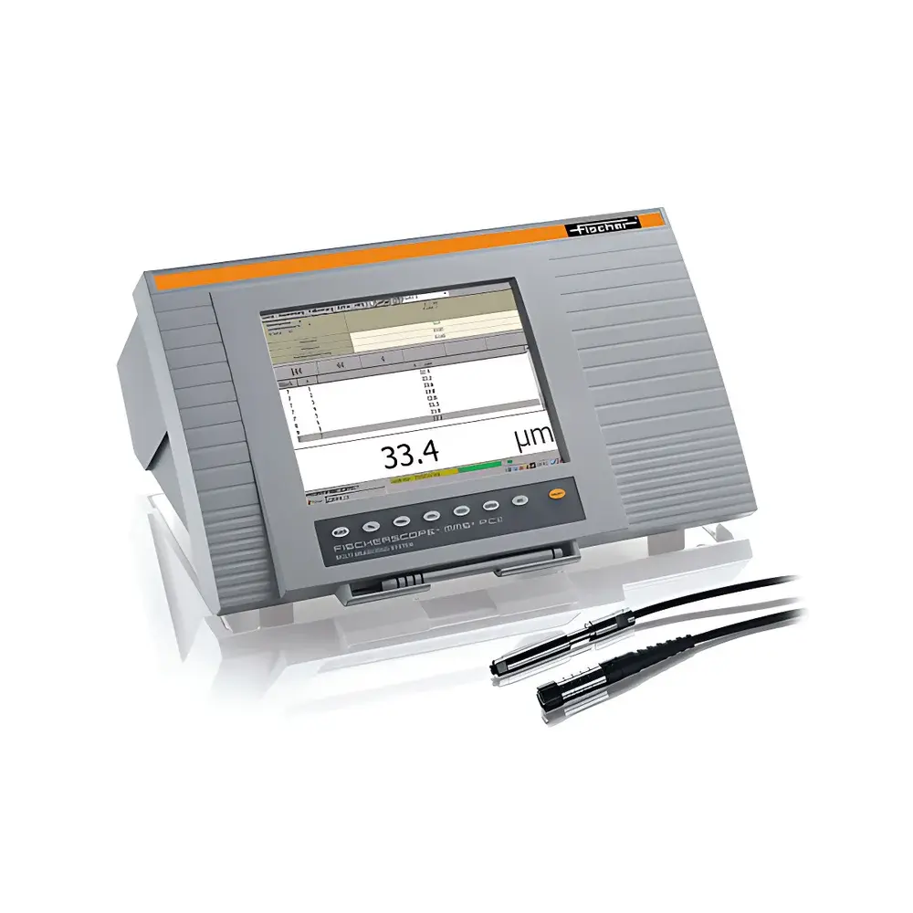
Fischer MMS PC2 BU Desktop Copper Thickness Tester
| Origin | Germany |
|---|---|
| Manufacturer Type | Authorized Distributor |
| Origin Category | Imported |
| Model | MMSPC-2 |
| Price Range | USD 28,000 – 70,000 |
Overview
The Fischer MMS PC2 BU is a high-precision desktop instrument engineered for non-destructive measurement of copper foil thickness on bare printed circuit board (PCB) substrates. It operates on the four-point probe micro-resistivity principle—also known as the Kelvin sensing method—where current is injected through two outer electrodes while voltage is sensed across two inner electrodes, eliminating lead resistance and contact potential errors. This methodology ensures traceable, repeatable quantification of surface copper thickness in the range of 5 µm to 120 µm, with resolution down to 0.1 µm, independent of underlying dielectric layers or backside copper presence. Designed for QC laboratories and PCB fabrication facilities, the system complies with IPC-TM-650 2.2.17 (measuring copper thickness on laminates) and supports metrological traceability to national standards via NIST-traceable calibration protocols.
Key Features
- 10.1-inch full-color capacitive touchscreen interface with intuitive icon-based navigation and multilingual support (including English, German, Chinese, and Japanese)
- Modular architecture based on the SR_SCOPE MMS PC1 plug-in module, enabling seamless integration of application-specific probe interfaces and signal conditioning electronics
- Dedicated PROBE ERCU N1 four-point contact probe optimized for bare copper foil on FR-4, polyimide, and ceramic substrates—immune to interference from adjacent conductive layers or ground planes
- Onboard storage for up to 1,000 user-defined measurement applications, each configurable with unique probe type, calibration curve, statistical limits, and pass/fail criteria
- Integrated data acquisition engine capable of storing over one million individual thickness readings with timestamp, location tag, operator ID, and environmental metadata (temperature/humidity if external sensors are connected)
- Real-time SPC functionality including X-bar/R charts, Cp/Cpk calculation, histogram generation, and out-of-control alarm triggers compliant with ISO 22514-2 and AIAG SPC manual requirements
- Standard communication interfaces: RS-232 (for legacy printer or PLC integration), USB 2.0 (host/device modes), Gigabit Ethernet (supporting DHCP, static IP, and SNMP v3), plus PS/2 ports for external keyboard and mouse
Sample Compatibility & Compliance
The MMS PC2 BU is validated for use on rigid and flexible PCBs with surface copper thicknesses ≥5 µm and substrate thicknesses from 0.05 mm to 3.2 mm. It accommodates standard panel sizes up to 450 × 600 mm when mounted on optional motorized XY stages (sold separately). Measurement repeatability is ≤±0.3% of reading (k=2) under controlled lab conditions (23 ± 1 °C, 50 ± 5% RH). The instrument meets IEC 61326-1:2013 for electromagnetic compatibility and IEC 61010-1:2010 for electrical safety. Software firmware complies with FDA 21 CFR Part 11 requirements for electronic records and signatures when operated in audit-trail-enabled mode, supporting role-based access control and immutable log archiving.
Software & Data Management
Fischer’s proprietary WinFTM® software (v5.8+) provides full remote control, report generation (PDF/CSV/XML), and database synchronization with enterprise LIMS or MES platforms via ODBC/JDBC drivers. All measurement sessions include automatic metadata tagging—date/time, operator credentials, calibration status, probe serial number, and environmental logs. Audit trails record every configuration change, calibration event, and data export action with digital signature verification. Export formats conform to ASTM E1447 and ISO/IEC 17025 reporting guidelines, including uncertainty budgets calculated per GUM (JCGM 100:2008).
Applications
- Final inspection of etched copper thickness on outer layers prior to solder mask application
- Verification of electrodeposited copper uniformity across HDI and IC substrate panels
- In-process monitoring of copper plating thickness during electrochemical deposition (ECD) process development
- Failure analysis of delamination-related thickness variation in multilayer flex circuits
- Supplier qualification testing per IPC-A-600 and IPC-6012 Class 2/3 acceptance criteria
- Process capability studies for copper thickness control in automotive ADAS and aerospace-grade PCB manufacturing
FAQ
What measurement principle does the PROBE ERCU N1 use, and why is it immune to backside copper influence?
It employs the four-terminal (Kelvin) resistivity method: current injection and voltage sensing occur at physically separated points, eliminating parasitic resistance from substrate or opposing copper layers.
Can the MMS PC2 BU be integrated into an automated production line?
Yes—via Ethernet/IP or Modbus TCP protocols; optional I/O expansion modules support discrete trigger signals, pneumatic actuator control, and PLC handshake logic.
Is calibration traceable to international standards?
All factory calibrations are performed using NIST-traceable copper foil standards (SRM 2135a/b) and documented per ISO/IEC 17025 requirements.
Does the system support GLP/GMP-compliant operation?
When configured with WinFTM® in “Regulatory Mode”, it enforces electronic signatures, audit trails, and 21 CFR Part 11–compliant data integrity controls.
What is the minimum measurable copper thickness on a 0.1 mm FR-4 substrate?
5 µm, provided surface roughness Ra ≤ 0.8 µm and no oxidation or organic contamination is present on the copper surface.


