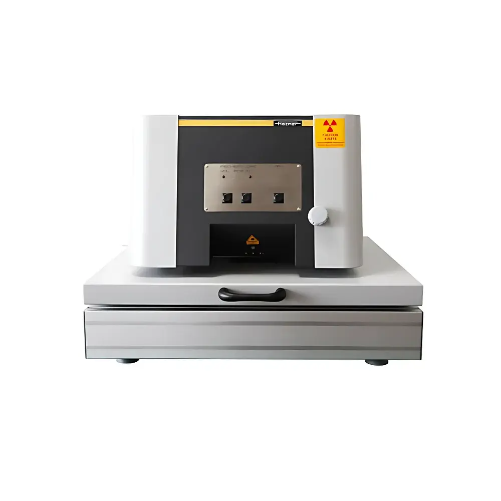
Fischer PCB200 X-ray Fluorescence Thickness Analyzer
| Origin | Germany |
|---|---|
| Manufacturer Type | Authorized Distributor |
| Origin Category | Imported Instrument |
| Model | PCB200 |
| Price Range | USD 68,000 – 136,000 |
Overview
The Fischer PCB200 is a benchtop energy-dispersive X-ray fluorescence (EDXRF) thickness analyzer engineered specifically for non-destructive, quantitative measurement of metallic coating thicknesses and elemental composition on printed circuit boards (PCBs). Operating on the fundamental principle of characteristic X-ray emission—where primary X-rays excite atoms in the sample, inducing secondary (fluorescent) X-rays whose energy and intensity are element-specific—the PCB200 delivers traceable, repeatable results for single- and multi-layer electroplated finishes including Cu, Ni, Sn, Au, Ag, Pd, and their alloys. Designed as an entry-level yet robust solution for QC labs and PCB fabrication facilities, it balances analytical performance with operational simplicity, supporting routine inspection without requiring dedicated radiation safety infrastructure beyond standard lab shielding protocols.
Key Features
- Integrated coaxial laser pointer for rapid, visual alignment of measurement position on irregular or densely populated PCB substrates
- Motorized drawer-style sample stage (PCB200 variant) enabling intuitive loading and precise Z-axis repeatability within ±2 µm
- High-resolution color CCD camera (1.3 MP) with real-time on-screen magnification and crosshair overlay for sub-millimeter positioning accuracy
- Optimized X-ray optics with Peltier-cooled Si-PIN detector and high-stability microfocus X-ray tube (50 kV max, 1 mA)
- Pre-calibrated factory reference standards traceable to NIST and BAM certified materials
- Compliance-ready hardware architecture supporting audit trails, user access levels, and electronic signature functionality per FDA 21 CFR Part 11 requirements
Sample Compatibility & Compliance
The PCB200 accommodates rigid and flexible PCBs up to 300 × 300 mm in footprint and 50 mm in height—including solder mask–coated, via-filled, and edge-plated specimens. Its collimated beam diameter (default 0.3 mm, optional 0.1 mm and 0.5 mm apertures) ensures spatial resolution suitable for measuring traces, pads, and plated-through holes without signal averaging from adjacent features. Analytical validation adheres to DIN ISO 3497 (Metallic coatings — Measurement of coating thickness — X-ray spectrometric methods) and ASTM B568 (Standard Test Method for Thickness Measurement of Metallic Coatings by X-Ray Spectrometry), with built-in uncertainty estimation based on counting statistics and matrix correction algorithms (Fundamental Parameters method). All calibration and verification procedures are documented in accordance with GLP and ISO/IEC 17025 laboratory accreditation frameworks.
Software & Data Management
Controlled exclusively via WINFTM® v5.x software (Windows 10/11 compatible), the PCB200 supports full workflow automation—from method setup and measurement execution to statistical reporting and SPC charting. The software includes customizable measurement templates for common PCB stack-ups (e.g., Cu/Ni/Au, Cu/Sn, ENIG), automatic peak deconvolution for overlapping spectral lines (e.g., Ni Kα and Cu Kβ), and integrated database management with SQL backend for long-term data archiving. Audit trail logs record operator ID, timestamp, parameter changes, and result exports; raw spectra and measurement metadata are stored in vendor-neutral .ftr and .csv formats to ensure interoperability with LIMS and enterprise QA systems.
Applications
- Thickness verification of immersion gold (ENIG), electroless nickel, immersion silver, and lead-free HASL finishes
- Quantitative analysis of alloy composition in solderable surface finishes (e.g., Sn–Pb vs. Sn–Ag–Cu)
- Process validation during electroplating bath maintenance and replenishment cycles
- Failure analysis of delamination, under-plating, or insufficient barrier layer deposition
- Supplier qualification testing per IPC-4552A (Electroless Nickel/Immersion Gold Plating Standard) and IPC-4556 (Immersion Silver)
FAQ
Does the PCB200 require external cooling or compressed air?
No—its X-ray tube and detector operate passively with integrated thermoelectric (Peltier) cooling and fan-assisted convection.
Can the instrument measure coatings on non-flat or warped PCBs?
Yes, the Z-height sensor and auto-focus algorithm compensate for sample tilt up to ±3°, and the drawer-stage design minimizes mechanical stress on fragile substrates.
Is spectral interference between Cu substrate and Ni plating corrected automatically?
Yes—WINFTM® applies matrix correction using Fundamental Parameters modeling, validated against certified multilayer reference standards.
What documentation is provided for regulatory audits?
Each unit ships with Factory Acceptance Test (FAT) report, ISO 17025-accredited calibration certificate, and IQ/OQ protocol templates compliant with GMP and IATF 16949 requirements.
How frequently must the instrument be recalibrated?
Annual recalibration is recommended; however, daily verification using onboard check standards satisfies most internal QA schedules per ISO 9001 clause 7.1.5.2.
")


