FISCHERSCOPE PMP10 PCB Copper Thickness Gauge
| Origin | Germany |
|---|---|
| Manufacturer Type | Authorized Distributor |
| Origin Category | Imported |
| Model | FISCHERSCOPE PMP10 |
| Pricing | Available Upon Request |
| Measurement Principle | Micro-Resistance (4-Point Probe) |
| Thickness Range | 0–120 µm |
| Accuracy | ±0.5 µm (5–50 µm), ≤1% of reading (50–80 µm), ≤2% of reading (>80 µm) |
| Test Area | 10 × 15 mm |
| Compliance | ISO 2178, ASTM B499, IPC-4552A, RoHS-compliant design |
Overview
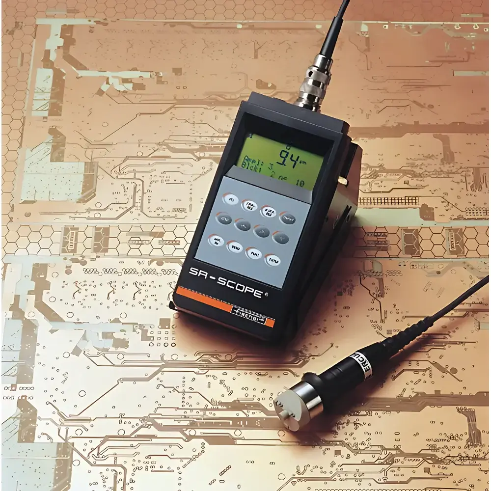
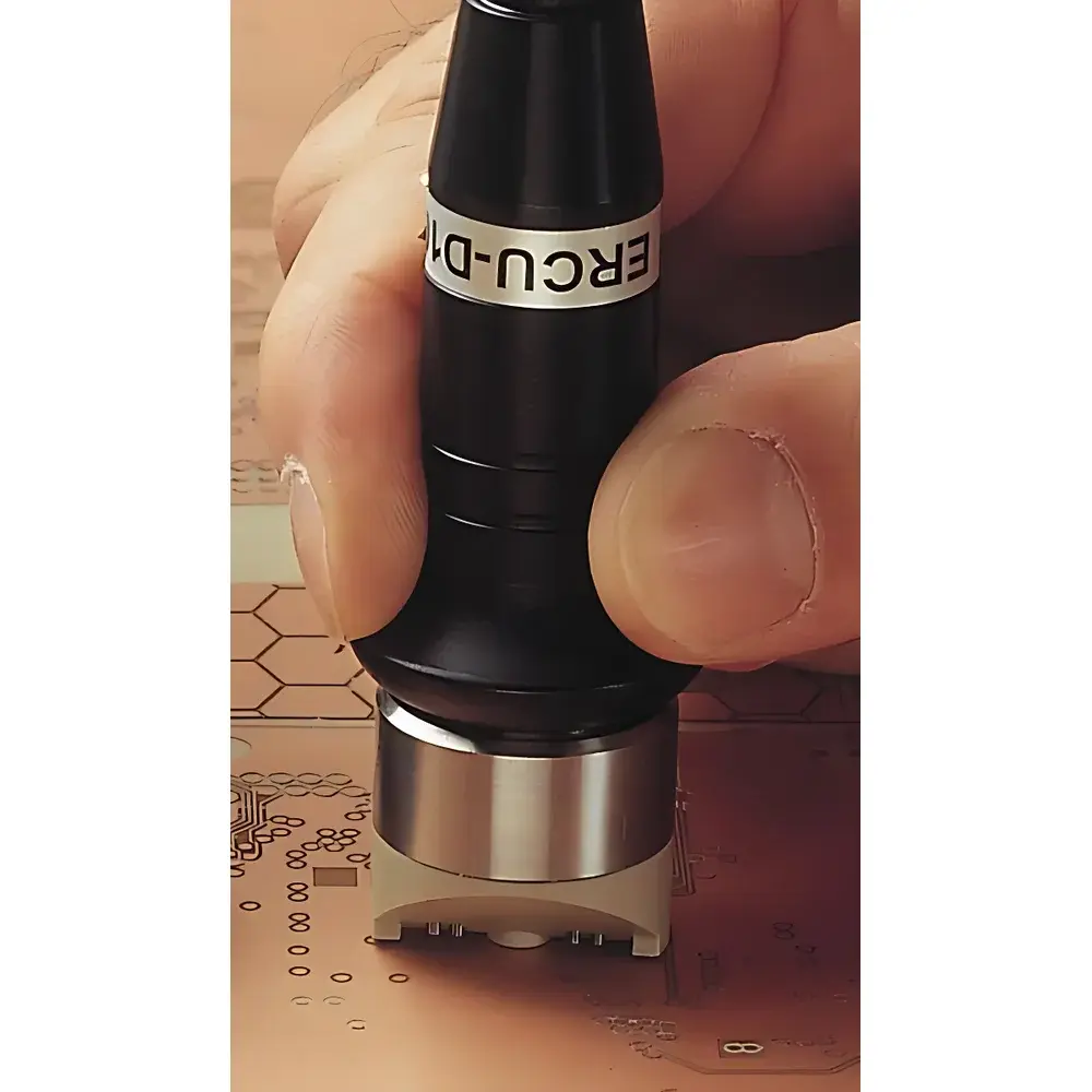
The FISCHERSCOPE PMP10 PCB Copper Thickness Gauge is a handheld, non-destructive micro-resistance measurement instrument engineered for precise, in-line quantification of copper layer thickness on printed circuit boards (PCBs). Unlike eddy-current or X-ray fluorescence (XRF) methods, the PMP10 employs a calibrated 4-point probe principle—applying a known current across two outer electrodes and measuring the voltage drop between two inner electrodes—to isolate surface copper resistivity and convert it directly to thickness with minimal influence from underlying conductive layers. This makes it uniquely suited for multilayer PCBs where backside copper, ground planes, or internal traces would otherwise distort readings. The device operates independently of substrate conductivity variations, enabling reliable measurements on FR-4, polyimide, ceramic, and flexible substrates—even when coated with solder mask, legend ink, or conformal coatings up to 100 µm thick.
Key Features
- True micro-resistance measurement architecture compliant with IPC-4552A Annex A for electrolytic and rolled copper verification
- Self-calibrating probe head with temperature-compensated electronics to maintain repeatability across ambient conditions (15–30 °C)
- Integrated 10 × 15 mm measurement footprint optimized for trace-width compatibility—supports evaluation of fine-pitch features down to 150 µm line/space
- Real-time statistical process control (SPC) output via USB or Bluetooth, including Cp/Cpk calculation per IPC-A-600 and IPC-6012 requirements
- Ruggedized industrial housing rated IP54, designed for cleanroom and production-floor deployment without external shielding
- On-device pass/fail thresholding with configurable alarm limits aligned to IPC Class 2 and Class 3 acceptance criteria
Sample Compatibility & Compliance
The PMP10 accommodates rigid, flex, and rigid-flex PCBs ranging from 0.1 mm to 3.2 mm in total thickness. It measures electrodeposited (ED), rolled annealed (RA), and reverse-treated copper foils without requiring substrate removal or cross-sectioning. Measurements remain stable across common solder mask chemistries—including liquid photoimageable (LPI), dry film, and UV-curable formulations—as long as coating thickness does not exceed 100 µm and exhibits uniform dielectric properties. The instrument conforms to ISO 2178 (non-magnetic coatings on magnetic substrates), ASTM B499 (magnetic and non-magnetic coatings on non-magnetic and magnetic base metals), and supports full audit trail generation required under ISO/IEC 17025-accredited laboratory workflows. Firmware includes built-in calibration certificate logging traceable to PTB (Physikalisch-Technische Bundesanstalt) reference standards.
Software & Data Management
The accompanying FISCHER WinFTM® software provides comprehensive data acquisition, visualization, and reporting capabilities. Users can define custom measurement templates per board layer stack-up, assign location-specific IDs (e.g., “Top Layer – Signal Trace Zone A”), and export timestamped datasets in CSV, PDF, or XML formats compatible with MES and ERP systems. All measurement sessions support FDA 21 CFR Part 11-compliant electronic signatures, role-based access control, and immutable audit trails—including operator ID, environmental sensor logs (temperature/humidity), probe calibration status, and raw voltage/resistance values. Data integrity is further ensured through SHA-256 hashing of each measurement record prior to database archiving.
Applications
- Final QA verification of outer-layer copper post-etch and plating processes
- In-process monitoring during pattern plating, HASL, ENIG, and ENEPIG surface finish deposition
- Failure analysis of blistering, delamination, or uneven copper distribution in HDI and IC substrates
- Process validation for additive manufacturing of embedded copper traces on polymer substrates
- Supplier qualification audits per IPC-6012 Rev G and IEC 61189-2 test method compliance
- DOE studies correlating etch rate uniformity with copper thickness gradients across panel dimensions
FAQ
Does the PMP10 require physical contact with bare copper?
No—measurements are valid through intact solder mask, silkscreen, and most standard conformal coatings, provided dielectric thickness remains within specification.
Can it distinguish between ED and RA copper morphology?
No—the PMP10 reports thickness only; microstructural differentiation requires SEM/EBSD or XRD analysis.
Is probe recalibration needed after every power cycle?
No—automatic zero-point compensation occurs at startup; full calibration is recommended every 30 days or after 500 measurements, per ISO/IEC 17025 guidelines.
What is the minimum measurable copper thickness?
The lower detection limit is 0.5 µm, validated using certified NIST-traceable thin-film standards.
How does it handle curved or warped PCB surfaces?
The spring-loaded probe head maintains consistent contact pressure (1.2 N ± 0.1 N) across surface deviations up to ±0.3 mm over the 10 × 15 mm aperture.


")
