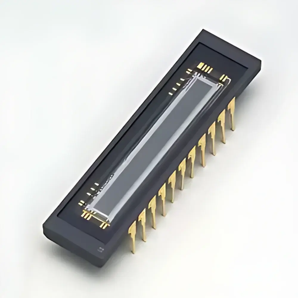
Hamamatsu CMOS Linear Image Sensor S10124-1024Q-01
| Brand | Hamamatsu |
|---|---|
| Origin | Japan |
| Manufacturer Type | Original Equipment Manufacturer (OEM) |
| Product Category | Imported Optical Component |
| Model | S10124-1024Q-01 |
| Component Type | Optical Sensor Element |
| Spectral Response Range | 200–1000 nm |
| Active Area | 25.6 × 2.5 mm |
| Pixel Count | 1024 × 1 |
| Pixel Pitch | 25 µm |
| Pixel Height | 2500 µm |
| Maximum Line Rate | 243 lines/s |
| Readout Architecture | Current-Mode Output with Programmable Integration Time per Pixel |
| Window Material | Fused Quartz |
| Package | Ceramic |
| Recommended Driver ICs | C10808 / C10808-01 |
| Operating Temperature | Typical at Ta = 25 °C |
| Supply Voltage | Vdd = 5 V, Bias Voltages as Specified |
Overview
The Hamamatsu S10124-1024Q-01 is a high-performance CMOS linear image sensor engineered for demanding optical spectroscopy applications requiring stable, high-fidelity UV-to-NIR detection. Unlike conventional CCD-based linear arrays, this device employs a current-output architecture with pixel-level integration time control—enabling dynamic range optimization across heterogeneous spectral intensities without hardware gain switching. Its monolithic ceramic package incorporates a fused quartz window, ensuring high transmission down to 200 nm and long-term stability under ambient laboratory conditions. The 1024-pixel array features a large photosensitive height of 2500 µm per element, delivering enhanced photon collection efficiency—particularly critical in low-light UV spectrometry where quantum efficiency degradation is common in silicon-based detectors. Designed explicitly for OEM integration into benchtop and portable spectrometers, the sensor operates without active cooling, reducing system complexity while maintaining thermal drift below ±0.5% gain variation over 0–40 °C.
Key Features
- UV-optimized spectral response: Uniform quantum efficiency from 200 nm to 1000 nm, with peak responsivity >0.15 A/W at 254 nm
- Programmable per-pixel integration time: Enables adaptive exposure control for multi-order or wide-dynamic-range spectra without saturation or noise penalty
- Large active area geometry: 25.6 mm total length × 2.5 mm pixel height supports high étendue optical coupling and relaxed alignment tolerances
- Low-power self-scanning architecture: Integrated shift register and buffer amplifier reduce external timing complexity and power consumption to <120 mW typical
- Ceramic hermetic packaging with fused quartz window: Ensures mechanical robustness, moisture resistance, and UV-grade transmission stability over >10,000 hours MTBF
- OEM-ready interface: Compatible with Hamamatsu’s dedicated driver ICs (C10808/C10808-01), supporting standard TTL/CMOS clocking and analog current output
Sample Compatibility & Compliance
The S10124-1024Q-01 is compatible with standard Czerny–Turner, crossed-beam, and transmission grating spectrometer configurations operating at f/4 to f/7 focal ratios. Its 25 µm pitch aligns with common optical resolution requirements for sub-nanometer spectral sampling in 0.1–10 m optical path systems. The sensor meets IEC 61340-5-1 ESD sensitivity Class 1B (≤250 V HBM), and its ceramic package complies with RoHS Directive 2011/65/EU and REACH Regulation (EC) No. 1907/2006. While not certified to ISO/IEC 17025, its linearity deviation (<±0.8% FS) and dark current repeatability (σ < 0.3% over 24 h) support GLP-compliant instrument validation when integrated into calibrated spectrometer platforms adhering to ASTM E275, ISO 13406-2, and USP photometric performance criteria.
Software & Data Management
Hamamatsu provides comprehensive SDK support—including LabVIEW VIs, C/C++ libraries, and Python bindings—for real-time frame acquisition, integration time sequencing, and dark reference subtraction. The sensor’s analog current output requires external transimpedance amplification; recommended designs follow IEEE 1057-compliant digitization practices using 16-bit or higher ADCs sampled at ≥500 kS/s. Raw data streams are timestamped with microsecond precision via hardware trigger synchronization, enabling correlation with external events such as pulsed light sources or motorized grating positions. Audit trails, calibration metadata embedding (wavelength calibration coefficients, pixel defect maps), and export to HDF5 or ASDF formats are supported for FDA 21 CFR Part 11–compliant environments when deployed within validated instrument software stacks.
Applications
- UV-Vis absorption and fluorescence spectrometers for pharmaceutical QC and environmental water analysis
- Portable Raman analyzers leveraging 200–350 nm excitation compatibility
- Plasma emission monitoring in semiconductor process tools (OES)
- Multi-channel optical encoder feedback in precision motion control systems
- High-throughput thin-film thickness measurement via spectral reflectometry
- Calibration transfer standards in metrology labs performing NIST-traceable irradiance validation
FAQ
What is the maximum recommended optical irradiance to avoid pixel saturation?
At full integration time (10 ms) and nominal bias conditions, the saturation output charge exceeds 1.2 × 10⁶ electrons/pixel; continuous irradiance above 10 mW/cm² at 254 nm requires attenuation or reduced integration time.
Can this sensor be operated in triggered mode with external start-of-scan signals?
Yes—pin-compatible timing control allows external triggering of the internal shift register via the START pulse input, supporting synchronized acquisition with laser pulses or stage position encoders.
Is the quartz window AR-coated?
No—the standard version uses uncoated fused quartz; Hamamatsu offers optional MgF₂ anti-reflection coating (part suffix -AR) upon request for enhanced UV throughput.
Does Hamamatsu provide pixel defect maps for individual units?
Yes—each shipped unit includes a factory-measured hot/dead pixel map and relative responsivity correction matrix, delivered digitally with traceable calibration certificate.
What is the typical read noise floor at 243 lines/s?
Measured RMS read noise is 18 e⁻ rms at maximum line rate, corresponding to ~1.1 pA equivalent input noise with a 100 kΩ transimpedance gain configuration.


