Evaporation Source Materials (Customizable High-Purity Thin-Film Deposition Feedstock)
| Brand | Hefei Kejing |
|---|---|
| Origin | Anhui, China |
| Manufacturer Type | Authorized Distributor |
| Country of Origin | PRC |
| Model | Evaporation Source Materials |
| Pricing | Available Upon Request |
Overview
Evaporation Source Materials are high-purity elemental or compound feedstocks engineered for physical vapor deposition (PVD) processes—specifically thermal evaporation and electron-beam (e-beam) evaporation—in vacuum thin-film systems. These materials serve as the precursor source for depositing functional layers in semiconductor fabrication, optical coating, OLED manufacturing, photovoltaic device R&D, and advanced materials characterization. Unlike consumables with fixed geometries, these source materials are supplied in customizable bulk forms—typically as pellets, chips, rods, or custom-machined shapes—to ensure optimal thermal stability, uniform vapor flux, and minimal crucible interaction during high-temperature evaporation cycles. Their composition, purity (routinely ≥99.99% to ≥99.9999%, depending on grade), and microstructural homogeneity directly influence film stoichiometry, adhesion, crystallinity, and long-term process repeatability.
Key Features
- Material flexibility: Compatible with >120 elemental metals (e.g., Al, Cr, Ni, Ti, Ag, Au, Pt), oxides (e.g., SiO₂, TiO₂, ITO), fluorides (e.g., MgF₂, CaF₂), sulfides (e.g., ZnS), and complex alloys (e.g., NiCr, TiAl, CoFeB)
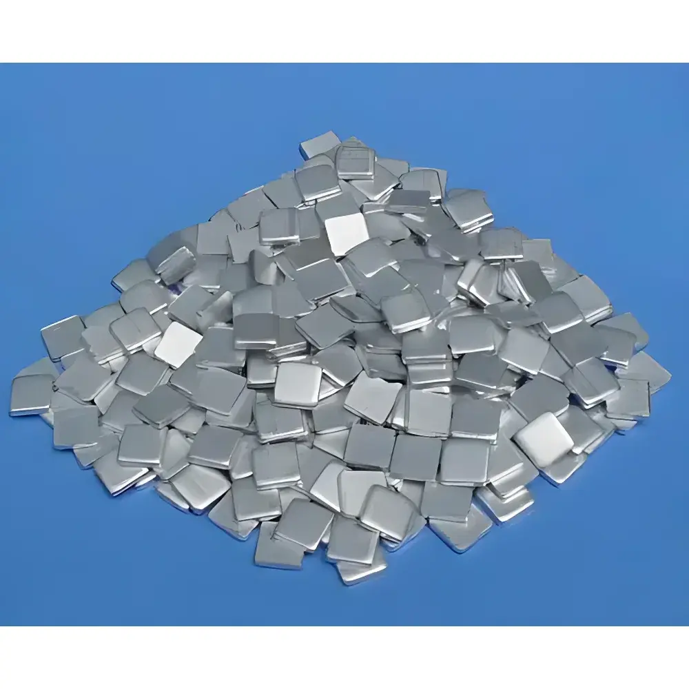
- Custom dimensional control: Standard form factor is ≈10 × 10 × 2 mm chip; thickness, planar geometry, aspect ratio, and crystallographic orientation can be specified per application requirements
- High-density sintering or zone-refined metallurgical processing available upon request to minimize porosity and volatile impurities
- Traceability documentation provided: Certificate of Analysis (CoA) includes ICP-MS and GDMS assay data, oxygen/nitrogen/hydrogen content (via LECO), and particle size distribution (for powder-derived forms)
- ISO 9001-certified packaging: Double-bagged under argon atmosphere in Class 1000 cleanroom conditions to prevent surface oxidation and particulate contamination
Sample Compatibility & Compliance
These evaporation materials are validated for use in standard planetary and linear e-beam sources (e.g., Temescal, SPECS, ULVAC), resistive-heated boats (Ta, Mo, W), and ceramic crucibles (BN, Al₂O₃). They meet material compatibility requirements defined in ASTM F1529 (Standard Guide for Selection of Materials for Vacuum Systems) and ISO 14644-1 (Cleanroom air cleanliness classification). For regulated environments—including medical device coating lines and pharmaceutical-grade thin-film sensor production—the materials support full traceability under ISO 13485 and FDA 21 CFR Part 820. Batch-specific CoAs and lot-level retention samples are retained for ≥5 years to satisfy GLP audit requirements.
Software & Data Management
While evaporation source materials themselves are passive components, their integration into automated deposition platforms (e.g., Kurt J. Lesker Auto 500, Angstrom Engineering APEX) relies on standardized material database protocols. Each batch is assigned a unique QR-coded label linking to an internal ERP record containing spectral purity profiles, thermal expansion coefficients (CTE), vapor pressure curves (derived from NIST TRC data), and recommended evaporation rates (nm/s at specific temperature gradients). This metadata enables seamless import into process recipe management systems compliant with SEMI E10 (Definition and Measurement of Equipment Reliability and Maintainability) and supports digital twin modeling of deposition kinetics.
Applications
- Semiconductor front-end: Gate electrode stacks (TiN, TaN), barrier layers (TaN, TiW), and interconnect seed layers (Cu, Ru)
- Optoelectronics: Anti-reflective (MgF₂), high-reflection (Ag/Al + dielectric stack), and transparent conductive oxide (ITO, AZO) coatings for lasers, AR/VR waveguides, and photodetectors
- Research-scale thin-film batteries: LiCoO₂, LiFePO₄, and solid electrolyte (Li₃PO₄–Li₄SiO₄) cathode/anode precursors
- Quantum device fabrication: Superconducting Nb, NbN, and Al films for SQUIDs and transmon qubits requiring sub-ppm carbon/oxygen contamination control
- Calibration standards: Certified reference materials (CRMs) for XRF, SIMS, and ellipsometry instrument validation
FAQ
What purity grades are available for evaporation source materials?
Standard grades include 99.99% (4N), 99.995% (4N5), and 99.999% (5N); ultra-high-purity 99.9999% (6N) is offered for critical quantum and metrology applications with additional GDMS certification.
Can I request directional grain alignment for metallic evaporation chips?
Yes—single-crystal or columnar-grain-oriented forms are available for refractory metals (e.g., Mo, W) and Ni-based superalloys upon submission of crystallographic axis specifications (e.g., [100], [110]).
Do you provide evaporation rate data for specific source-to-substrate configurations?
Rate data is provided in tabular and CSV format for standard source geometries (e.g., 10 mm diameter e-beam hearth, 25 mm source-to-substrate distance) under 1×10⁻⁶ Torr base pressure; custom modeling using Monte Carlo vapor transport simulation is available upon technical consultation.
Are these materials suitable for reactive evaporation processes (e.g., O₂ or N₂ co-evaporation)?
Yes—oxygen- and nitrogen-compatible variants (e.g., Ti, Al, Zr) are pre-conditioned to stabilize surface oxide/nitride nucleation sites, minimizing arcing and plasma instability during reactive deposition.
What documentation accompanies each shipment?
Each order includes a Certificate of Analysis (CoA), Material Safety Data Sheet (MSDS/SDS), ISO 9001 traceability statement, and batch-specific packaging log confirming argon purge integrity and cleanroom handling records.


