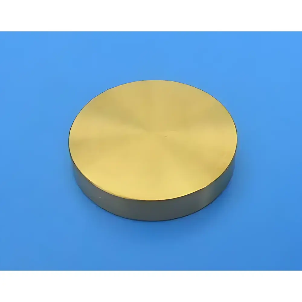
Hefei Kejing Au Sputtering Target
| Brand | Hefei Kejing |
|---|---|
| Origin | Anhui, China |
| Manufacturer Type | Authorized Distributor |
| Origin Category | Domestic (China) |
| Model | Au Target |
| Purity | 99.99% (4N) |
| Standard Dimensions | 10 × 10 × 2.0 mm, Ø20 × 2.0 mm, Ø30 × 3.0 mm, Ø80 × 0.5 mm |
| Packaging | Class 1000 Cleanroom + Class 100 Clean Bag |
| Pricing | Upon Request |
Overview
The Hefei Kejing Au Sputtering Target is a high-purity metallic thin-film deposition material engineered for physical vapor deposition (PVD), specifically direct-current (DC) and radio-frequency (RF) magnetron sputtering processes. Composed of elemental gold with certified 99.99% (4N) purity, this target meets stringent requirements for optical coatings, semiconductor interconnects, biosensor electrodes, and calibration standards in surface science instrumentation. Its precisely controlled stoichiometry, low oxygen and carbon impurity content (<5 ppm each), and uniform microstructure ensure consistent plasma ignition, stable deposition rates, and minimal arcing during extended sputtering runs. Designed for compatibility with standard vacuum chamber configurations—including 2-inch, 3-inch, and 4-inch target holders—the Au target supports both planar and rotatable cathode geometries. All units undergo post-processing annealing to relieve residual stress and improve thermal stability under high-power operation (up to 10 W/cm² continuous duty).
Key Features
- High-purity gold (99.99% minimum, verified by GDMS and ICP-MS) with trace metal impurities fully documented in CoA
- Precision-machined dimensional tolerances: ±0.05 mm thickness control, ±0.1 mm diameter/edge tolerance
- Surface finish: Ra ≤ 0.4 µm on sputtering face; double-side polished option available upon request
- Grain structure optimized for uniform erosion profile—average grain size 20–50 µm per ASTM E112
- Thermal conductivity ≥ 315 W/(m·K) at 25°C, enabling efficient heat dissipation during high-rate deposition
- Backside bonding interface compatible with indium, tin, or epoxy-based target mounting systems
Sample Compatibility & Compliance
This Au target is validated for use with substrates including silicon wafers (Si , ), fused silica, quartz, sapphire, ITO-coated glass, and flexible polymer films (e.g., PET, PI). It complies with ISO 14644-1 Class 5 (Class 100) cleanroom handling protocols during final packaging. Documentation includes full traceability to raw material lot, batch-specific impurity analysis reports, and conformance to SEMI F57-0218 (specification for sputtering targets). While not subject to FDA regulation as a finished device, the material satisfies USP particulate matter limits when used in medical-grade coating applications. All shipments include a Certificate of Conformance referencing ASTM F2627-20 (Standard Specification for Gold Sputtering Targets).
Software & Data Management
As a passive consumable component, the Au sputtering target does not incorporate embedded firmware or software interfaces. However, its performance metrics—including deposition rate stability, film thickness uniformity (±3.5% over 100 mm Ø), and sheet resistance reproducibility—are fully integrable into industry-standard thin-film process control platforms such as Applied Materials Endura® data logging modules, Angstrom Engineering COMPACT® system controllers, and custom LabVIEW-based deposition monitoring suites. Users may import target-specific parameters (purity, density, thermal expansion coefficient) into simulation tools like VIKING™ or DYNAMO® for predictive sputter yield modeling. Full traceability records are retained per ISO 9001:2015 clause 8.5.2, supporting GLP/GMP audit readiness.
Applications
- Optical thin-film stacks: IR reflectors, plasmonic nanostructure seeding layers, anti-reflection coating adhesion promoters
- Microelectronics: Ohmic contacts for GaAs and InP devices, bond pad metallization, MEMS electrode fabrication
- Biomedical research: Electrochemical biosensor working electrodes, SPR substrate functionalization, cell culture interface coatings
- Calibration standards: Reference materials for XPS quantification, TEM sample preparation, and AFM tip coating
- Research-grade photovoltaics: Back-contact layers for organic and perovskite solar cells requiring low-work-function interfaces
FAQ
What is the typical target lifetime under DC sputtering at 100 W?
Target lifetime depends on chamber geometry, pressure, and cooling efficiency; under standardized conditions (5 mTorr Ar, water-cooled cathode, 100 W DC), expect ≥ 80 kWh of cumulative energy delivery before >15% erosion depth.
Can this Au target be bonded to a copper backing plate?
Yes—standard indium solder bonding is recommended; alternative options include low-temperature eutectic alloys (e.g., Bi–Sn) or conductive epoxies meeting IPC-4101D Class A specifications.
Is vacuum-outgassing data available?
Yes—TDS (thermal desorption spectroscopy) data shows total mass loss <0.08% at 200°C for 24 h, with H₂O and CO₂ as dominant evolved species.
Do you offer custom alloyed Au targets (e.g., Au–Pt or Au–Ni)?
Custom compositions are available through our R&D partnership program; lead time is typically 8–12 weeks from specification approval.
Are RoHS and REACH declarations provided with shipment?
Yes—each batch includes a compliant declaration referencing EU Directive 2011/65/EU Annex II and SVHC candidate list version current at date of manufacture.


 System")