KEJING MgO Single Crystal Substrates for Thin-Film Deposition
| Brand | KEJING |
|---|---|
| Origin | Anhui, China |
| Manufacturer Type | Authorized Distributor |
| Product Origin | Domestic (China) |
| Model | MgO |
| Price | Upon Request |
| Crystal Structure | Cubic |
| Lattice Constant | a = 4.216 Å |
| Growth Method | Arc Melting |
| Melting Point | 2850 °C |
| Density | 3.58 g/cm³ |
| Mohs Hardness | 5.5 |
| Thermal Expansion Coefficient | 12.8 × 10⁻⁶ /°C |
| Dielectric Constant | 9.8 |
| Optical Transmission | >90% @ 200–400 nm, >98% @ 500–1000 nm |
| Cleavage Plane | <100> |
| Standard Orientations | <100>, <110>, <111> |
| Orientation Tolerance | ±0.5° |
| Surface Roughness | Ra < 5 Å (<100> & <110>), Ra < 15 Å (<111>) |
| Polishing | Single-Side or Double-Side CMP |
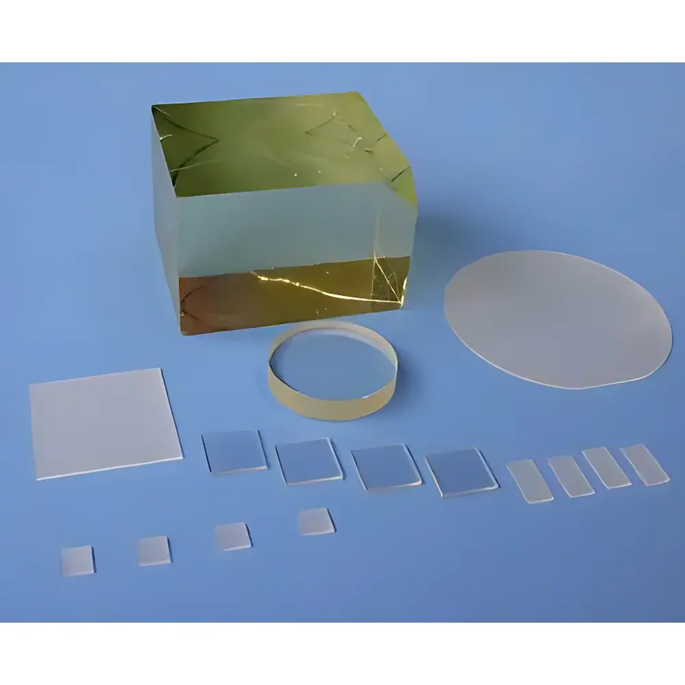
| Available Sizes | 10 × 10 × 0.5 mm, 5 × 5 × 0.5 mm, Ø1″ × 0.5 mm, Ø2″ × 0.5 mm |
Overview
KEJING MgO single crystal substrates are high-purity, orientation-controlled cubic oxide wafers engineered for epitaxial thin-film growth in advanced functional materials research and industrial device fabrication. As a dielectric substrate with low microwave loss (tan δ < 0.0003 at 10 GHz) and exceptional thermal stability, MgO serves as a foundational platform for depositing high-temperature superconducting (HTS) films such as YBCO and BSCCO, ferroelectric oxides (e.g., PZT, SBT), magnetic perovskites (e.g., LSMO), and optoelectronic heterostructures. Its lattice mismatch with common HTS compounds is minimized through precise orientation control, enabling atomically coherent interfacial growth critical for microwave filter performance in 5G base stations and satellite communication systems. The substrates are grown via controlled arc melting—a technique ensuring stoichiometric fidelity and low defect density—followed by chemical-mechanical polishing (CMP) to achieve atomic-level surface flatness (Ra < 5 Å) and monolayer step-terrace morphology essential for molecular beam epitaxy (MBE) and pulsed laser deposition (PLD).
Key Features
- High-purity MgO crystals (>99.99% trace metal basis), verified by GDMS and secondary ion mass spectrometry (SIMS)
- Cubic crystal structure with lattice parameter a = 4.216 Å, matched to perovskite and fluorite-type film lattices
- Low dielectric loss tangent across RF to millimeter-wave bands (1–100 GHz), supporting high-Q resonator design
- Thermally robust up to 2850 °C; compatible with high-temperature annealing (>800 °C) under oxidizing or vacuum atmospheres
- Precision orientation tolerance of ±0.5°, certified by high-resolution X-ray diffraction (HR-XRD) rocking curve analysis
- Atomically smooth surfaces: Ra < 5 Å for and orientations; Ra < 15 Å for , measured by AFM over 5 × 5 µm² areas
- Available in industry-standard dimensions including Ø2″ (50.8 mm) wafers—enabling scalable sputtering and PLD processes
Sample Compatibility & Compliance
These substrates are routinely employed in UHV-compatible thin-film systems operating under pressures ≤1×10⁻⁸ Torr. Their low outgassing rate (<1×10⁻¹² Torr·L/s·cm² after bakeout at 300 °C) ensures minimal contamination during epitaxial growth. All wafers undergo rigorous cleaning per SEMI F57 standards and are packaged in Class 100 cleanroom environments using static-dissipative, particle-free polypropylene wafer carriers or nitrogen-purged 100-grade laminar flow bags. Documentation includes full traceability reports (batch ID, growth log, XRD data, surface metrology), supporting GLP-compliant R&D workflows and ISO/IEC 17025-accredited laboratory validation.
Software & Data Management
While MgO substrates themselves are passive components, KEJING provides digital substrate passports accessible via secure customer portal. Each batch includes downloadable calibration files for XRD peak indexing, AFM topography datasets (Gwyddion-compatible .gws format), and optical transmission spectra (200–1200 nm, resolution 1 nm). Integration with thin-film process control software (e.g., SENTECH Instrumentation’s SENTECH-ICP, Oxford Instruments’ PLD Control Suite) is supported through standardized CSV metadata templates compliant with ASTM E2812-21 for substrate characterization reporting.
Applications
- Epitaxial growth of YBa₂Cu₃O₇₋δ (YBCO) for high-performance HTS microwave bandpass filters and multiplexers
- Deposition of SrTiO₃ buffer layers on MgO for lattice-matched integration with complex oxide heterostructures
- Template-assisted growth of spintronic devices based on La₀.₇Sr₀.₃MnO₃ (LSMO) and Fe₃O₄ on -oriented MgO
- UV-transparent substrate for deep-UV photodetectors and AlGaN-based optoelectronics (200–280 nm range)
- Reference standard for ellipsometry calibration and dielectric spectroscopy benchmarking (1 kHz–10 MHz)
FAQ
What is the typical surface finish specification for -oriented MgO substrates?
Standard single-side polished MgO wafers exhibit Ra < 5 Å over 5 × 5 µm² scan areas, with step-terrace height uniformity ≤0.4 nm (monolayer precision) confirmed by tapping-mode AFM.
Can KEJING provide custom off-axis orientations (e.g., 4° miscut)?
Yes—custom miscut angles from 0.1° to 6.0° are available with full XRD verification and surface step characterization; lead time increases by 3–4 weeks.
Are these substrates suitable for use in reactive sputtering environments with oxygen plasma?
Absolutely. MgO demonstrates excellent chemical inertness under O₂ plasma (up to 500 W, 5 Pa) and maintains surface integrity without stoichiometric deviation or surface roughening after 120 min exposure.
Do you supply substrates with pre-deposited seed layers (e.g., CeO₂ or YSZ buffers)?
KEJING offers optional e-beam evaporated CeO₂ (5–20 nm) or RF-sputtered YSZ (10–50 nm) buffer layers with in-situ RHEED monitoring; all buffer-coated substrates include cross-sectional TEM certification.
How is crystal orientation verified prior to shipment?
Each wafer undergoes ω-2θ and φ-scan XRD on a Bruker D8 Discover system; orientation report includes full pole figure maps, FWHM values (<0.15° for ), and lattice parameter deviation from reference (±0.002 Å).