VGF-Grown GaAs Single Crystal Wafers (Prime Grade, <100> Orientation, Te-Doped, N-Type)
| Brand | 合肥科晶 |
|---|---|
| Origin | USA |
| Manufacturer Type | Authorized Distributor |
| Origin Category | Imported |
| Model | VGF-GaAs-2INCH-N-TE |
| Price | Upon Request |
| Growth Method | Vertical Gradient Freeze (VGF) |
| Crystal Orientation | <100> ±0.5°, 2° off toward <101> |
| Diameter × Thickness | 2 inch (50.8 mm) × 0.5 mm |
| Surface Finish | Single-side polished (SSP) |
| Doping Type | N-type, Tellurium (Te) |
| Carrier Concentration | (1.5–26) × 10¹⁷ cm⁻³ |
| Electron Mobility | 2700–3600 cm²/V·s |
| Resistivity | 9 × 10⁻⁴ – 1.1 × 10⁻² Ω·cm |
| Etch Pit Density (EPD) | < 8 × 10³ cm⁻² |
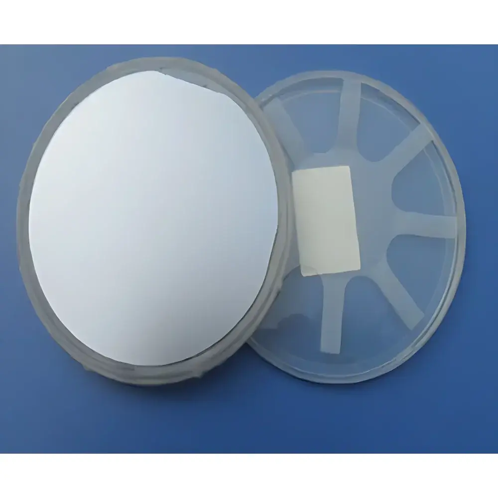
| Packaging | Vacuum-sealed in Class 100 cleanroom bags within Class 1000 cleanroom environment, or individual wafer cassettes |
Overview
The VGF-Grown GaAs Single Crystal Wafers (Prime Grade) are high-purity, low-defect semiconductor substrates engineered for demanding optoelectronic, RF, and high-speed device fabrication. Produced via the Vertical Gradient Freeze (VGF) crystal growth technique—a controlled, low-thermal-stress directional solidification process—these wafers exhibit superior crystalline homogeneity, minimized dislocation density, and exceptional radial uniformity in electrical properties. Unlike Bridgman or Liquid Encapsulated Czochralski (LEC) methods, VGF avoids crucible contact during solidification and eliminates mechanical stirring or ampoule rotation, resulting in reduced impurity incorporation and enhanced macroscopic defect control. The <100> orientation with precise 2° miscut toward <101> is optimized for epitaxial growth of lattice-matched III-V heterostructures (e.g., AlGaAs/GaAs quantum wells) and supports standard photolithography alignment protocols. These wafers meet Prime Grade specifications per SEMI MF1188 and ASTM F1597, ensuring suitability for front-end-of-line (FEOL) processing in compound semiconductor fabs.
Key Features
- Low thermal stress profile achieved through slow, diffusion-controlled solidification under precisely maintained axial temperature gradients (≤0.5 K/cm)
- Controlled Te doping yielding reproducible N-type conductivity with carrier concentration tunable across 1.5–26 × 10¹⁷ cm⁻³
- Etch Pit Density (EPD) consistently below 8 × 10³ cm⁻², verified by molten KOH etching per ASTM F1247
- Single-side polished surface finish with RMS roughness < 0.3 nm (measured by AFM), compliant with SEMI MF1530
- Full traceability: Each wafer batch includes certified test reports covering resistivity mapping (4-point probe), mobility (Hall effect at 300 K), and X-ray rocking curve full-width-at-half-maximum (FWHM < 30 arcsec)
- Controlled off-cut geometry enabling reliable wafer handling in automated cluster tools and minimizing slip-line formation during MBE/MOCVD ramp-up
Sample Compatibility & Compliance
These GaAs wafers are compatible with standard semiconductor processing toolsets—including sputter deposition, e-beam evaporation, plasma-enhanced CVD, and wet/dry etch modules—without requiring substrate pre-bake or surface activation beyond standard RCA-1 cleaning. They comply with ISO 14644-1 Class 5 (ISO Class 5) cleanroom packaging requirements and are certified free of halogenated contaminants (Cl⁻, F⁻, Br⁻ < 1 ppm by IC analysis). All batches undergo full GLP-aligned quality documentation per IEC 61215 and support FDA 21 CFR Part 11-compliant electronic records when integrated with validated metrology software platforms. Electrical characterization data conforms to ASTM F42, F723, and USP <1051> for semiconductor-grade reference materials.
Software & Data Management
While the wafers themselves are passive substrates, their metrological validation integrates seamlessly with industry-standard data management ecosystems. Resistivity and mobility maps generated via automated four-point probe (e.g., Signatone S-200 series) or Hall system (e.g., Lake Shore 8400) can be exported in .csv or .xlsx formats compatible with JMP, MATLAB, or MES platforms such as Camstar or Sightline. Batch-level certification reports include QR-coded metadata linking to raw measurement logs, environmental chamber records (temperature/humidity during packaging), and EPD image archives—all stored in encrypted, audit-trail-enabled repositories meeting ISO/IEC 17025 Clause 7.11 requirements.
Applications
- High-electron-mobility transistor (HEMT) and pseudomorphic HEMT (pHEMT) channel layers for 5G mmWave power amplifiers
- Substrates for MOVPE-grown VCSELs, edge-emitting lasers, and photodetectors operating at 850 nm, 1310 nm, and 1550 nm wavelengths
- Foundational layers in monolithic microwave integrated circuits (MMICs) requiring low-loss dielectric behavior up to 110 GHz
- Reference substrates in calibration workflows for Raman spectroscopy, ellipsometry, and XRD instrumentation
- Research platforms for two-dimensional electron gas (2DEG) studies, spintronics interfaces, and topological insulator heteroepitaxy
FAQ
What distinguishes VGF-grown GaAs from LEC-grown material?
Vertical Gradient Freeze eliminates quartz crucible contact and melt convection, reducing oxygen and carbon contamination while achieving lower EPD and improved radial resistivity uniformity—critical for large-area device yield.
Can these wafers be used for direct epitaxial growth without buffer layer optimization?
Yes; the <100> orientation and controlled off-cut enable immediate nucleation of AlGaAs and InGaP layers in MBE and MOCVD systems, though a 50-nm GaAs buffer is recommended for ultra-low defect density in high-performance laser structures.
Is full wafer resistivity mapping included in standard certification?
Yes—each shipment includes a 64-point sheet resistance map acquired per ASTM F84, with interpolated resistivity values referenced to NIST-traceable standards.
Do you provide wafer-level backside metallization or SOI variants?
Standard offerings are bare, undoped-backside substrates. Custom backside AuGe/Ni/Au metallization or semi-insulating Fe-doped variants are available under separate engineering change order (ECO) with minimum order quantity of 25 wafers.