CdTe Crystal Substrates
| Brand | Hefei Kejing |
|---|---|
| Origin | Anhui, China |
| Manufacturer Type | Authorized Distributor |
| Origin Category | Domestic (China) |
| Model | CdTe Crystal Substrate |
| Pricing | Upon Request |
| Crystal Structure | Cubic F43m, Lattice Constant a = 6.483 Å |
| Growth Method | Physical Vapor Transport (PVT) |
| Melting Point | 1047 °C |
| Density | 5.851 g/cm³ |
| Specific Heat Capacity | 0.210 J/g·K |
| Thermal Expansion Coefficient | 5.0 × 10⁻⁶ /K |
| Thermal Conductivity (300 K) | 6.3 W/m·K |
| Transmission Range | 0.85–29.9 µm |
| Refractive Index (at 10.6 µm) | 2.72 |
| Standard Orientations | <100>, <001>, <110>, <111> |
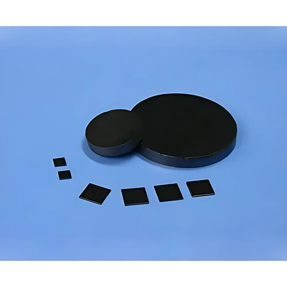
| Standard Dimensions | 5 × 5 × 0.5 mm, 10 × 10 × 0.5 mm, Ø25.4 × 0.5 mm |
| Packaging | Class 1000 Cleanroom Handling, Class 100 Clean Bag or Individual Protective Cassette |
Overview
CdTe (Cadmium Telluride) crystal substrates are single-crystal wafers engineered for high-performance optoelectronic and radiation detection applications. As a II–VI compound semiconductor with a direct bandgap of ~1.44 eV at room temperature, CdTe exhibits exceptional X-ray and gamma-ray stopping power, low dark current, and broad mid- to far-infrared transparency—making it a material of choice for high-resolution spectroscopic detectors, infrared windows, and epitaxial templates for HgCdTe (MCT) growth. These substrates are grown via the Physical Vapor Transport (PVT) method under controlled stoichiometric conditions to minimize Te inclusions and vacancy-related defects, ensuring high crystalline perfection and reproducible optical homogeneity across batches. The cubic F43m crystal structure (space group No. 216) provides isotropic thermal expansion and consistent lattice matching for heteroepitaxy, while its refractive index of 2.72 (measured at 10.6 µm) supports anti-reflection coating design for CO₂ laser optics and thermal imaging systems.
Key Features
- High-purity single-crystal CdTe with dislocation density < 1 × 10⁴ cm⁻² (verified by X-ray topography)
- Controlled orientation options: , , , and planes—each polished to ≤0.2 nm RMS surface roughness (Ra) using chemical-mechanical polishing (CMP)
- Thermal stability up to 1047 °C with low coefficient of thermal expansion (5.0 × 10⁻⁶ /K), enabling compatibility with high-temperature thin-film deposition processes
- Broadband IR transmission from 0.85 µm (near-IR edge) to 29.9 µm (far-IR cutoff), validated per ASTM E1421 for infrared transmittance measurement
- Robust mechanical handling: Vickers hardness ≈ 40 HV, fracture toughness ~0.5 MPa·m¹/², suitable for vacuum-compatible mounting and sputter-coating fixtures
- Class 1000 cleanroom fabrication environment with final packaging in ISO Class 5 (100-class) laminar flow bags or individual static-dissipative cassettes
Sample Compatibility & Compliance
CdTe substrates are compatible with molecular beam epitaxy (MBE), metalorganic chemical vapor deposition (MOCVD), and pulsed laser deposition (PLD) systems used in III–V and II–VI heterostructure fabrication. Their lattice parameter (a = 6.483 Å) enables near-lattice-matched growth of Hg₁₋ₓCdₓTe layers for high-operating-temperature (HOT) infrared focal plane arrays. All substrates comply with ISO 10110-7 for optical surface quality and meet ASTM F1529 requirements for semiconductor substrate dimensional tolerances. Trace metal impurity levels (Fe, Cu, Ni, Cr) are maintained below 1 × 10¹⁵ atoms/cm³ per secondary ion mass spectrometry (SIMS) analysis. While not certified to IEC 61215 or UL 1703, these substrates are routinely qualified for use in GLP-compliant detector module assembly lines serving medical imaging and nuclear safeguards applications.
Software & Data Management
Each substrate batch is accompanied by a Certificate of Conformance (CoC) containing full metrological data: orientation verification via Laue X-ray diffraction, surface flatness (PV ≤ λ/10 @ 633 nm), thickness uniformity (±0.01 mm), and spectral transmittance curves (2–20 µm, measured on Bruker Vertex 80v FTIR). Raw spectral datasets and XRD pole figures are provided in ASCII format compliant with ASTM E1317 data exchange standards. For traceability in regulated environments, optional audit-ready documentation includes lot-specific QC records aligned with FDA 21 CFR Part 11 electronic signature requirements—available upon request for customers operating under GMP or ISO 13485 quality management systems.
Applications
- X-ray and gamma-ray spectroscopy detectors in medical CT, PET/CT hybrid systems, and homeland security portal monitors
- Infrared optical components: windows, beamsplitters, and ATR crystals for FTIR spectroscopy and thermal imaging lenses
- Epitaxial templates for MCT-based infrared photodetectors operating at 77–150 K
- Substrates for thin-film solar cell research (e.g., CdTe/CdS heterojunctions) and photoelectrochemical water-splitting studies
- Calibration standards for synchrotron beamline diagnostics and THz time-domain spectroscopy setups
FAQ
What crystal orientations are available, and how is orientation verified?
Standard orientations include , , , and , confirmed via back-reflection Laue diffraction with angular accuracy ±0.2°. Orientation reports are included with each shipment.
Can custom thicknesses or non-standard dimensions be supplied?
Yes—custom geometries (e.g., 15 × 15 × 1.0 mm, rectangular blanks with beveled edges, or wafer-scale formats) are available subject to minimum order quantity and lead time confirmation.
Is polycrystalline CdTe offered, and what are its typical applications?
Polycrystalline CdTe substrates are available for cost-sensitive R&D applications such as bulk radiation sensor prototyping and evaporative source crucibles—contact technical sales for grain size distribution and resistivity specifications.
What surface finish options are supported?
Standard finish is double-side polished (DSP) with 1–5 nm RMS roughness; optional etch-and-polish (E&P) or epitaxial-ready (EP) finishes with atomically flat terraces (<0.1 nm step height) are available upon request.
How are substrates packaged to ensure contamination control during shipping?
All substrates are sealed in nitrogen-purged, static-dissipative Class 100 clean bags inside rigid foam-lined boxes. Custom packaging (e.g., dry nitrogen-filled glovebox-compatible containers) can be arranged for high-sensitivity applications.