NdGaO3 Single Crystal Substrate Wafers by Hefei Kejing
| Key | Brand: Hefei Kejing |
|---|---|
| Origin | Anhui, China |
| Crystal Structure | Orthorhombic |
| Lattice Parameters | a = 5.43 Å, b = 5.50 Å, c = 7.71 Å |
| Melting Point | 1600 °C |
| Density | 7.57 g/cm³ |
| Dielectric Constant | 25 |
| Growth Method | Czochralski (Cz) |
| Orientation Tolerance | ±0.5° |
| Surface Finish | Single-side polished, Ra < 0.5 nm |
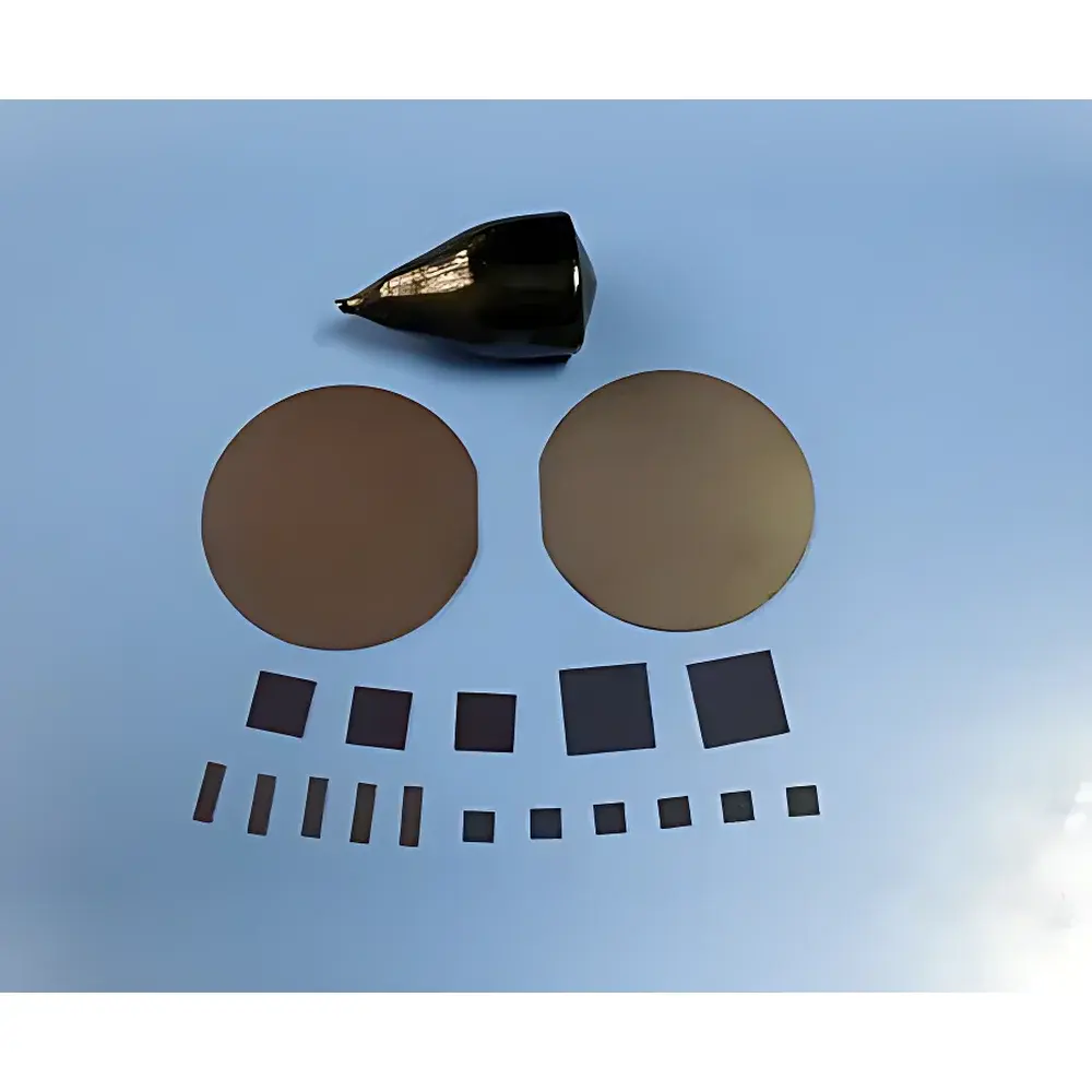
| Standard Dimensions | 10 × 10 × 0.5 mm, 10 × 5 × 0.5 mm, 5 × 3 × 0.5 mm |
| Available Orientations | <001>, <110>, <100> |
| Packaging | Class 1000 cleanroom processed, sealed in Class 100 clean bags |
Overview
NdGaO₃ (neodymium gallate) single crystal substrates are engineered orthorhombic perovskite-structured wafers designed for high-precision epitaxial thin-film deposition in advanced materials research. Developed over the past decade as an alternative to conventional substrates such as SrTiO₃ or LaAlO₃, NdGaO₃ exhibits exceptional lattice matching with high-temperature superconducting oxides—particularly YBa₂Cu₃O₇₋δ (YBCO)—with a measured lattice mismatch of only ~0.27%. Its structural stability across wide temperature ranges (no phase transitions below 1600 °C), combined with low thermal expansion anisotropy and high dielectric constant (εᵣ ≈ 25), makes it ideal for fabricating atomically ordered heterostructures in oxide electronics, spintronics, and quantum interface studies. The substrate’s robust mechanical integrity and chemical inertness under oxygen-rich annealing conditions further support reproducible MBE (molecular beam epitaxy) and PLD (pulsed laser deposition) growth protocols.
Key Features
- High-purity single-crystal structure grown via the Czochralski method, ensuring low defect density and uniform stoichiometry.
- Precise crystallographic orientation control (, , and ) with angular tolerance ≤ ±0.5°, verified by high-resolution X-ray diffraction (HR-XRD).
- Single-side polished surface finish with root-mean-square roughness (Ra) < 0.5 nm, enabling monolayer-level epitaxial registry during film nucleation.
- Thermally stable up to 1600 °C and chemically resistant to common oxidizing atmospheres used in post-growth annealing (e.g., O₂ at 1 atm, 600–800 °C).
- Available in standardized dimensions (10 × 10 × 0.5 mm, 10 × 5 × 0.5 mm, 5 × 3 × 0.5 mm) with custom sizing and orientation options upon request.
- Class 1000 cleanroom processing and double-bagged packaging in Class 100 clean polyethylene pouches minimize particulate and hydrocarbon contamination prior to loading into UHV deposition systems.
Sample Compatibility & Compliance
NdGaO₃ substrates are routinely employed in ultra-high vacuum (UHV) thin-film synthesis platforms compliant with ISO 14644-1 Class 5 (ISO Class 5) cleanroom integration standards. Their compatibility extends to industry-standard epitaxial techniques including pulsed laser deposition (PLD), molecular beam epitaxy (MBE), and sputter-based reactive deposition. The material meets ASTM F1913 specifications for crystalline oxide substrate dimensional tolerances and surface quality. While not certified under FDA 21 CFR Part 11 or GLP/GMP frameworks—given its role as a passive substrate rather than a regulated analytical component—it is documented per ISO/IEC 17025 traceability guidelines when supplied with full certificate of analysis (CoA), including XRD rocking curve FWHM data, surface profilometry reports, and EDX elemental mapping.
Software & Data Management
As a passive crystalline substrate, NdGaO₃ does not incorporate embedded firmware or require proprietary software. However, its use in automated deposition systems (e.g., Riber, PVD Products, or custom-built PLD clusters) integrates seamlessly with standard process control interfaces—including LabVIEW-based acquisition modules and EPICS-compatible PLC logic—for synchronized substrate temperature ramping, shutter sequencing, and real-time pressure monitoring. All characterization datasets (XRD θ–2θ scans, AFM topographs, RHEED oscillation traces) generated using NdGaO₃ substrates are fully compatible with open-format scientific data standards (HDF5, TIFF, .xy) and can be imported into commercial analysis suites such as Jade, Gwyddion, or Igor Pro for quantitative epitaxial quality assessment.
Applications
- Epitaxial growth of YBCO and other cuprate superconductors for Josephson junction arrays and SQUID sensors.
- Integration of complex oxide heterostructures (e.g., LSMO/NdGaO₃, LCMO/NdGaO₃) for magnetoelectric coupling studies.
- Template layer for ferroelectric domain engineering in BiFeO₃ and Pb(Zr,Ti)O₃ films.
- Substrate for interfacial superconductivity investigations in two-dimensional electron gases (2DEGs) formed at oxide interfaces.
- Reference platform in comparative thin-film strain analysis, leveraging its well-characterized elastic constants and thermal expansion coefficients.
FAQ
What is the typical off-axis angle specification for NdGaO₃ substrates?
Standard orientations are cut to within ±0.5° of nominal Miller indices; tighter tolerances (±0.1°) are available upon request with additional metrology verification.
Can NdGaO₃ substrates be reused after thin-film growth?
Reuse is generally not recommended due to irreversible surface reconstruction, interdiffusion, or residual carbon/oxygen contamination following high-temperature processing; virgin substrates are advised for quantitative reproducibility.
Is HF etching compatible with NdGaO₃?
Hydrofluoric acid is strongly discouraged—NdGaO₃ contains Ga–O bonds susceptible to HF-induced pitting and non-stoichiometric leaching; buffered oxide etch (BOE) or dilute HCl-based cleans are preferred for pre-deposition surface activation.
Do you provide XRD rocking curve data with each batch?
Yes—certificates of analysis include full ω-scan FWHM values (typically < 0.15° for wafers) and reciprocal space mapping (RSM) summaries upon customer request.
Are larger formats (e.g., 15 mm diameter) available?
Custom diameters and thicknesses (up to 1.0 mm) are supported; lead time increases by 4–6 weeks for non-standard geometries requiring re-sawing and re-polishing.


")