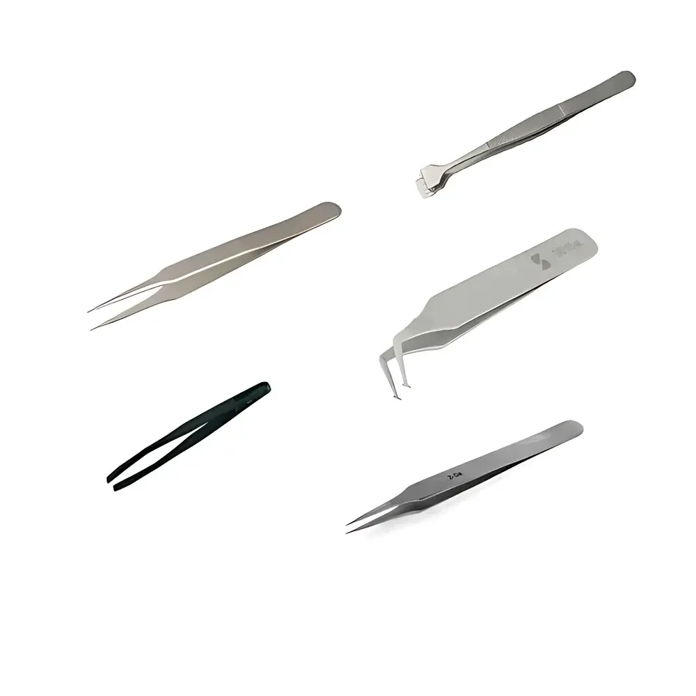
Kojin Substrate Tweezers Series
| Brand | Kojin |
|---|---|
| Origin | Anhui, China |
| Manufacturer Type | Authorized Distributor |
| Product Origin | Domestic (China) |
| Model Series | Substrate Tweezers Series |
| Core Application Domain | Semiconductor & Optical Component Handling |
| Material Compatibility | Si wafers, fused silica, sapphire, CaF₂, BK7, and other precision optical substrates |
| ESD Compliance | Available in static-dissipative and fully antistatic configurations |
| Construction | Stainless steel (304/316), carbon fiber, or beryllium copper variants |
| Tip Finishing | Electropolished, diamond-lapped, or PTFE-coated options |
| Tip Width Range | 0.05 mm to 2.0 mm |
| Operating Environment | Class 10–100 cleanrooms, vacuum chambers (≤10⁻⁶ mbar), and gloveboxes |
Overview
The Kojin Substrate Tweezers Series is a purpose-engineered family of precision handling tools designed for the non-destructive manipulation of fragile, high-value optical and semiconductor substrates under controlled laboratory and production environments. Unlike general-purpose forceps, these tweezers are engineered to minimize mechanical stress, surface scratching, particle generation, and electrostatic discharge—critical failure modes during wafer transfer, thin-film deposition setup, optical alignment, and vacuum-integrated metrology workflows. Each variant adheres to dimensional tolerances ≤±1.5 µm at the tip apex and undergoes rigorous metrological verification per ISO 9001-certified protocols. The series supports both manual and semi-automated integration into cleanroom-compatible tooling stations, including load-lock interfaces and robotic end-effectors.
Key Features
- Substrate-specific tip geometry: Silicon wafer tweezers feature 15° tapered, mirror-polished tips optimized for and crystal plane engagement without edge chipping; optical component tweezers incorporate radius-matched concave profiles for lens and prism handling.
- Multi-material platform: Selectable base materials include austenitic stainless steel (ASTM F138-compliant), beryllium copper (for enhanced ESD control and fatigue resistance), and carbon fiber-reinforced polymer (for magnetic-free operation in interferometry setups).
- ESD-safe architecture: Antistatic models integrate surface resistivity control (10⁴–10⁶ Ω/sq) via conductive polymer coatings or embedded carbon nanotube networks, validated per ANSI/ESD S20.20 and IEC 61340-5-1.
- Vacuum compatibility: Electropolished variants meet ASTM B912 standards for passivation and are rated for continuous operation in UHV environments (10⁻⁷ Pa) without outgassing or particulate shedding (tested per ISO 14644-1 Class 10 certification).
- Modular tip exchange system: Interchangeable tips (sold separately) enable rapid reconfiguration between silicon, quartz, and metalized substrate handling without recalibration or cross-contamination risk.
Sample Compatibility & Compliance
The Kojin Substrate Tweezers Series accommodates substrates ranging from 50 mm (2″) to 300 mm (12″) diameter wafers, as well as irregularly shaped optical elements—including plano-convex lenses, etalons, diffraction gratings, and MEMS mirrors. All models comply with SEMI F20-0303 (semiconductor equipment materials) and ISO 10110-7 (optical element handling). ESD-rated variants support full traceability under FDA 21 CFR Part 11 requirements when paired with Kojin’s optional digital logbook module. Cleanroom suitability is certified per ISO 14644-1 Class 10 and JIS B 9920:2019.
Software & Data Management
While inherently mechanical, the tweezers integrate seamlessly into digitally auditable workflows via optional RFID-enabled handles (Kojin TW-RFID-HL-200). Each unit carries a unique serialized tag storing calibration history, last sterilization timestamp (autoclave or plasma cycle), and material compatibility matrix. When scanned at process gates, logs synchronize with LabVantage LIMS or Thermo Fisher SampleManager platforms, supporting GLP/GMP audit trails and preventive maintenance scheduling based on cumulative actuation cycles.
Applications
- Transfer of bare and patterned Si, GaAs, InP, and SOI wafers between cassette loaders, spin coaters, and e-beam lithography stages.
- Positioning of AR-coated fused silica windows and MgF₂ prisms during laser cavity assembly in Class 10 cleanrooms.
- Handling of delicate perovskite and organic photovoltaic substrates during glovebox-based device fabrication.
- Metrology sample mounting for spectral ellipsometry, white-light interferometry, and X-ray reflectivity measurements.
- Repair and rework of micro-opto-electro-mechanical systems (MOEMS) where sub-50 µm feature integrity must be preserved.
FAQ
Are these tweezers compatible with automated wafer handling robots?
Yes—models with standardized 8-mm hex drive shanks (e.g., KST-SS-120-HEX) are mechanically and electrically interfaced with Brooks AutoMate™, MKS Sigma™, and KLA TeraScan™ robotic arms.
Do you provide calibration certificates traceable to NIM or NIST?
Calibration reports per ISO/IEC 17025 are available upon request; tip geometry verification uses Zeiss Axio Imager.M2m with 200× differential interference contrast imaging.
Can the tips be autoclaved or plasma-cleaned?
Stainless steel and beryllium copper variants withstand 121°C/2 bar autoclaving (EN 285); PTFE-coated tips require low-temperature plasma (O₂/Ar, 100 W, 5 min) per ASTM F2657.
What is the maximum recommended operating temperature?
Standard models: 150°C continuous; high-temp variants (KST-BE-CU-HT) rated to 300°C for MBE source effusion cell loading.
Is there a warranty covering tip deformation under normal use?
Kojin offers a 24-month limited warranty against manufacturing defects; tip wear due to abrasive substrate contact falls under consumable replacement guidelines (recommended replacement after 10,000 gripping cycles).


