合肥科晶 Nb:SrTiO₃ (Niobium-Doped Strontium Titanate) Single-Crystal Substrates — High-Conductivity Cubic Perovskite Wafers for Electrochemical and Thin-Film Device Fabrication
| Brand | Hefei Kejing |
|---|---|
| Origin | Anhui, China |
| Manufacturer Type | Authorized Distributor |
| Product Category | Domestic |
| Model | Nb:SrTiO₃ |
| Crystal Structure | Cubic, a = 3.905 Å |
| Growth Method | Verneuil |
| Density | 5.175 g/cm³ |
| Melting Point | 2080 °C |
| Mohs Hardness | 6 |
| Thermal Expansion Coefficient | 10.4 × 10⁻⁶ /°C |
| Resistivity | 0.007 Ω·cm (0.7 wt% Nb), 0.08 Ω·cm (0.1 wt% Nb) |
| Loss Tangent (tan δ) | ~5 × 10⁻⁴ at 10 GHz, 300 K |
| Surface Finish | Single- or Double-Polished, Ra < 5 nm |
| Orientation Tolerance | <100> ± 0.5° |
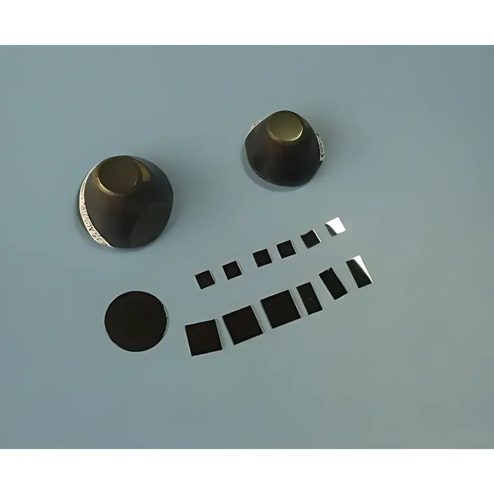
| Standard Dimensions | 10 × 10 × 0.5 mm, 5 × 5 × 0.5 mm |
Overview
Nb:SrTiO₃ (niobium-doped strontium titanate) single-crystal substrates are engineered perovskite wafers designed for applications requiring both structural lattice matching and tunable electronic conductivity. Unlike insulating SrTiO₃, Nb doping introduces n-type carriers into the TiO₂ sublattice, transforming the material from a wide-bandgap dielectric (Eg ≈ 3.2 eV) into a degenerate semiconductor with resistivity controllable between 10⁻³ and 10⁻¹ Ω·cm—depending on dopant concentration (0.001–0.7 wt% Nb). This enables direct integration as conductive bottom electrodes in oxide heterostructures, solid-state electrochemical cells, and high-frequency piezoelectric or dielectric thin-film devices. The cubic symmetry (space group Pm3̄m), low dielectric loss, and thermal expansion compatibility with common functional oxides (e.g., La₀.₇Sr₀.₃MnO₃, YBa₂Cu₃O₇, BaTiO₃) make Nb:SrTiO₃ an established platform for epitaxial growth via pulsed laser deposition (PLD), sputtering, and molecular beam epitaxy (MBE). All substrates are grown by the Verneuil method under controlled oxygen partial pressure to ensure stoichiometric reproducibility and minimal point defect clustering.
Key Features
- High-purity, orientationally precise single crystals with ± 0.5° alignment—certified by X-ray rocking curve full-width at half-maximum (FWHM) ≤ 0.05°
- Controlled Nb doping (0.001–0.7 wt%) enabling tailored bulk resistivity without compromising crystallinity or surface integrity
- Ultra-smooth surface finish: Ra < 5 nm (measured by atomic force microscopy), available in single- or double-polished configurations for optimal nucleation uniformity
- Thermally stable up to 2080 °C with coefficient of thermal expansion (10.4 × 10⁻⁶ /°C) closely matched to LSCO, STO, and LSMO layers—reducing interfacial strain during high-temperature processing
- Chemically inert in ambient air and aqueous environments; resistant to standard etchants used in microfabrication (e.g., dilute HF, buffered oxide etch)
- Low microwave dielectric loss: tan δ ≈ 5 × 10⁻⁴ at 10 GHz and 300 K—suitable for RF/microwave device integration and impedance spectroscopy calibration standards
Sample Compatibility & Compliance
Nb:SrTiO₃ substrates are routinely employed in GLP-compliant thin-film development workflows and meet baseline requirements for ISO/IEC 17025-accredited materials characterization labs. Their defined crystallographic orientation, surface roughness, and resistivity traceability support standardized protocols for electrode interface studies per ASTM F2628 (Standard Guide for Evaluating Electrical Properties of Oxide Thin Films) and IEC 62471 (Photobiological Safety of Lamps and Lamp Systems) when used in optoelectronic test structures. Each wafer batch is accompanied by a Certificate of Conformance specifying orientation verification (XRD θ–2θ scan), surface roughness (AFM), and four-point probe resistivity data. No hazardous substances are introduced during polishing or packaging; substrates comply with RoHS Directive 2011/65/EU Annex II restrictions.
Software & Data Management
While Nb:SrTiO₃ substrates themselves are passive components, they serve as foundational elements in instrumented thin-film systems—including quartz crystal microbalance (QCM) setups, electrochemical impedance spectroscopy (EIS) cells, and in situ synchrotron XRD chambers. When integrated into automated deposition platforms (e.g., PLD or sputter systems), substrate identifiers (lot number, orientation, thickness) are logged into LabArchives or Benchling ELN instances via barcode scanning. For metrology traceability, surface topography (AFM), crystal quality (XRD rocking curves), and sheet resistance (four-point probe mapping) datasets are archived in vendor-agnostic HDF5 format, compatible with Python-based analysis pipelines (e.g., SciPy, scikit-image) and MATLAB-based thin-film modeling tools (e.g., WVASE, DeltaPsi2).
Applications
- Bottom electrodes for resistive switching memristors and ferroelectric tunnel junctions (FTJs)
- Conductive templates for epitaxial growth of complex oxides in quantum materials research (e.g., 2D electron gases at LAO/STO interfaces)
- Reference substrates in QCM-D (quartz crystal microbalance with dissipation monitoring) for real-time adsorption kinetics of biomolecules on conductive oxide surfaces
- Electrochemical sensor platforms for pH, NO₂, or O₂ detection in solid-state electrolyte configurations
- Dielectric spacers in gate-tunable oxide field-effect transistors (OFETs) operating at cryogenic temperatures
- Calibration standards for terahertz time-domain spectroscopy (THz-TDS) and microwave cavity perturbation measurements
FAQ
What is the typical carrier concentration range achievable in Nb:SrTiO₃ substrates?
Carrier density ranges from ~10¹⁹ cm⁻³ (0.1 wt% Nb) to ~10²⁰ cm⁻³ (0.7 wt% Nb), confirmed by Hall effect measurements at 300 K.
Are custom orientations or thicknesses available beyond standard specifications?
Yes—custom cuts along , , or off-axis orientations (±0.1° tolerance), as well as thicknesses from 0.3 mm to 1.0 mm, are available upon request with lead times of 6–8 weeks.
Do you provide pre-cleaned substrates suitable for UHV deposition?
All substrates undergo plasma cleaning (O₂/Ar) immediately prior to packaging and are sealed in Class 100 cleanroom bags; full cleaning protocols (RCA, piranha, annealing) are documented in the technical datasheet.
Is there batch-to-batch resistivity variation, and how is it controlled?
Resistivity deviation across a production lot is maintained within ±8% via in-line four-point probe screening and post-growth secondary ion mass spectrometry (SIMS) dopant profiling.
Can these substrates be used for electrochemical impedance spectroscopy (EIS) without additional metallization?
Yes—the intrinsic conductivity eliminates the need for sputtered Au or Pt electrodes; however, edge-contact geometry must be optimized to minimize series resistance contributions in low-frequency (<1 Hz) measurements.