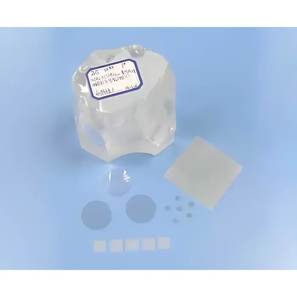
Zirconia (YSZ) Single-Crystal Substrates
| Brand | Hefei Kejing |
|---|---|
| Origin | Anhui, China |
| Manufacturer Type | Authorized Distributor |
| Origin Category | Domestic |
| Model | YSZ Single-Crystal Substrate |
| Pricing | Upon Request |
| Chemical Formula | (Zr,Y)O₂ (Zr:Y = 91:9) |
| Crystal Structure | Cubic |
| Lattice Constant | a = 5.125 Å |
| Density | 5.8 g/cm³ |
| Purity | 99.99% |
| Melting Point | 2800 °C |
| Thermal Expansion Coefficient | 10.3 × 10⁻⁶ /°C |
| Dielectric Constant | 27 |
| Growth Method | Arc Melting |
| Orientations Available | <100>, <110>, <111> (±0.5° tolerance) |
| Standard Dimensions | Ø2" × 0.5 mm, 10 × 10 × 0.5 mm, 10 × 5 × 0.5 mm |
| Surface Finish | Single- or Double-Polished, Ra < 5 Å |
| Packaging | Class 1000 Cleanroom Assembly, Sealed in Class 100 Clean Bags or Individual Protective Cassette Boxes |
Overview
Zirconia (YSZ) single-crystal substrates are high-purity, orientation-controlled piezoelectric and electrochemically inert platforms engineered for use in quartz crystal microbalance (QCM) systems, solid oxide fuel cell (SOFC) sensor development, high-temperature electrochemical impedance spectroscopy (EIS), and thin-film epitaxial growth applications. Yttria-stabilized zirconia (YSZ) is synthesized by doping ZrO₂ with ~9 mol% Y₂O₃ to retain the cubic fluorite structure at ambient and elevated temperatures—eliminating destructive phase transitions observed in pure zirconia. This structural stabilization enables long-term mechanical integrity, chemical resistance to acidic/alkaline environments, and thermal stability up to 2800 °C. The cubic lattice (a = 5.125 Å) provides uniform atomic spacing critical for reproducible electrode deposition and interfacial charge-transfer studies. These substrates serve as foundational elements in QCM-based mass-sensing platforms where frequency shift (Δf) correlates directly with nanogram-level mass changes on the crystal surface via the Sauerbrey equation.
Key Features
- Ultra-high purity (99.99%) single-crystal YSZ grown via controlled arc melting—ensuring low defect density and minimal grain boundary scattering
- Precise crystallographic orientation (, , or ) with angular tolerance ≤ ±0.5°, enabling orientation-dependent electrochemical and piezoelectric characterization
- Surface roughness Ra < 5 Å achieved through single- or double-side polishing—critical for uniform thin-film adhesion and low-noise QCM operation
- Thermal expansion coefficient (10.3 × 10⁻⁶ /°C) closely matched to common electrode materials (e.g., Pt, Au, Ni), minimizing interfacial stress during thermal cycling
- High dielectric constant (εᵣ ≈ 27) and low dielectric loss—supporting stable capacitive coupling in impedance-based sensing configurations
- Robust chemical inertness in oxidizing, reducing, and corrosive atmospheres up to 1000 °C—validated per ISO 14644-1 cleanroom handling protocols
Sample Compatibility & Compliance
YSZ substrates are compatible with standard QCM electrode sputtering (e.g., Au, Pt, Ir), ALD/PVD thin-film deposition, and high-temperature annealing in tube furnaces under O₂, N₂, H₂, or forming gas. All substrates are processed and packaged in ISO Class 5 (100) cleanroom environments and sealed in static-dissipative, particle-free packaging to meet ASTM F2459-22 requirements for semiconductor-grade substrates. Orientation verification is performed using X-ray diffraction (XRD) with Cu-Kα radiation; full certification includes lattice parameter confirmation, rocking curve FWHM ≤ 0.15°, and surface contamination screening via TOF-SIMS. Documentation supports GLP-compliant traceability including lot-specific certificates of analysis (CoA), material safety data (MSDS), and cleanroom handling logs.
Software & Data Management
While YSZ substrates themselves are passive components, they integrate seamlessly into QCM-D (quartz crystal microbalance with dissipation monitoring) systems from leading vendors (e.g., Biolin Scientific QSense, Malvern Panalytical) that support FDA 21 CFR Part 11–compliant audit trails, electronic signatures, and raw-data export in HDF5 or ASCII formats. When used in custom-built electrochemical cells, substrates support time-resolved impedance acquisition synchronized with temperature ramping (via Eurotherm or Watlow controllers), with metadata tagging for orientation, surface finish, and batch ID—enabling cross-experiment reproducibility tracking in LIMS or ELN platforms (e.g., LabArchives, Benchling).
Applications
- Mass-sensitive detection of biomolecular adsorption (e.g., protein binding, DNA hybridization) in liquid-phase QCM biosensors
- High-temperature electrochemical gas sensing (CO, NOₓ, hydrocarbons) using YSZ-based potentiometric or amperometric cells
- Model substrate for epitaxial growth of functional oxides (e.g., LSM, LSCF, STO) in pulsed laser deposition (PLD) and sputtering systems
- Reference platform for calibrating AFM tip wear, nanoindentation modulus, and interfacial shear rheology in soft matter studies
- Dielectric layer in multilayer capacitors and MEMS resonators operating above 500 °C
FAQ
What crystal orientations are available, and how is orientation verified?
Standard options include , , and orientations, each certified via θ–2θ XRD scans and pole-figure mapping. Angular deviation is guaranteed within ±0.5°, with full XRD reports provided per batch.
Can these substrates be used in ultra-high vacuum (UHV) environments?
Yes—YSZ exhibits negligible outgassing below 10⁻¹⁰ mbar after bakeout at 400 °C for 2 hours, making them suitable for UHV-compatible QCM and MBE applications.
Is double-polishing necessary for QCM applications?
Double-polishing is recommended for symmetric electrode configurations (e.g., front/back Au electrodes) to ensure parallelism and minimize acoustic mode dispersion. Single-polish suffices for standard top-electrode-only setups.
Do you provide custom thicknesses or non-standard dimensions?
Custom thicknesses (0.2–2.0 mm) and planar dimensions (up to 50 × 50 mm) are available upon request; lead time and minimum order quantities apply.
How should YSZ substrates be cleaned prior to thin-film deposition?
A standard protocol includes sequential ultrasonication in acetone, isopropanol, and DI water (10 min each), followed by O₂ plasma treatment (100 W, 30 s) to remove organic residue without altering stoichiometry.