Titanium Dioxide (Anatase) Single Crystal Substrate –合肥科晶 OEM for US Sourcing
| Brand | Hefei Kejing |
|---|---|
| Origin | USA |
| Manufacturer Type | Authorized Distributor |
| Origin Category | Imported |
| Model | Anatase TiO₂ Single Crystal Substrate |
| Pricing | Available Upon Request |
| Crystallographic Orientations | <001>, <100>, <101>, <110>, <111> |
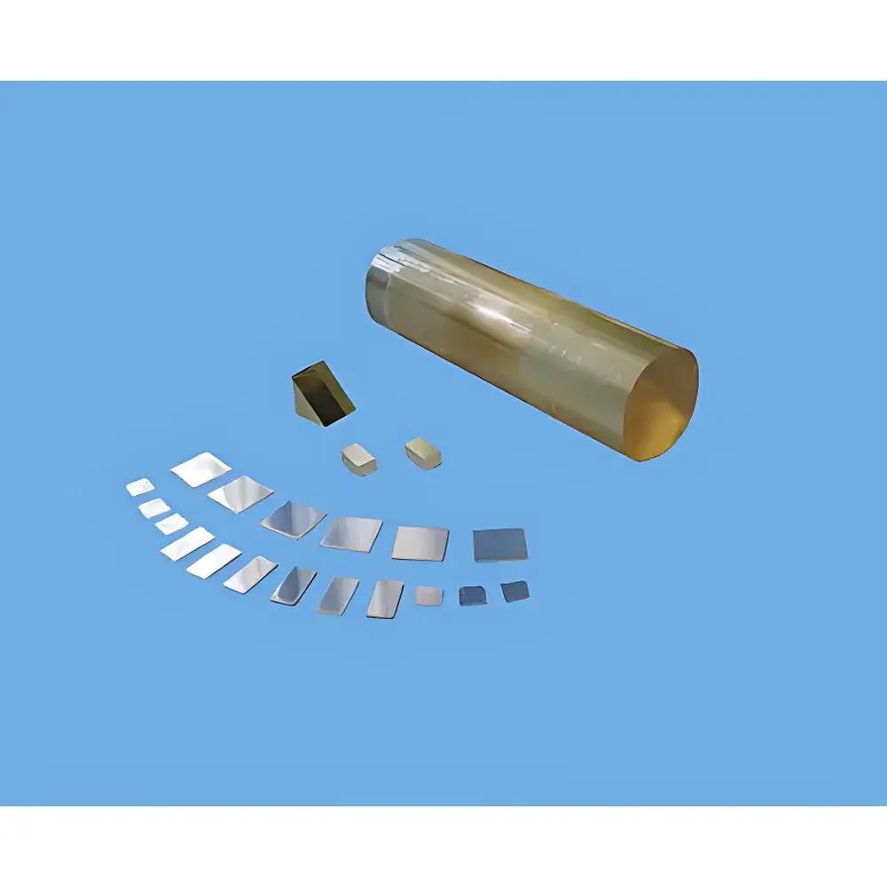
| Standard Dimensions | 5 × 5 × 0.5 mm |
| Surface Finish | Single-Side Polished (Ra < 0.3 nm) |
| Packaging | Class 1000 Cleanroom-Assembled in Class 100 Clean Bags |
Overview
Titanium dioxide (TiO₂) in its anatase polymorph is a wide-bandgap (≈3.2 eV) semiconductor with exceptional photocatalytic activity, high electron mobility, and strong surface reactivity under UV illumination. Unlike rutile or brookite phases, anatase exhibits superior charge carrier separation efficiency and lower recombination rates—making it the preferred single-crystal substrate for fundamental studies in surface science, photoelectrochemistry, oxide heteroepitaxy, and quantum confinement experiments. This product is a high-purity, orientation-controlled anatase TiO₂ single crystal substrate, sourced from U.S.-based crystal growth facilities and distributed under strict quality stewardship by Hefei Kejing Materials Technology Co., Ltd. Each wafer is grown via chemical vapor transport (CVT) or flux methods, followed by precision orientation verification using high-resolution X-ray diffraction (HR-XRD) and Laue back-reflection. The substrate serves as a foundational platform for atomic-layer deposition (ALD), molecular beam epitaxy (MBE), and scanning probe microscopy (SPM) applications requiring atomically defined surface terminations.
Key Features
- Phase-pure anatase structure confirmed by Raman spectroscopy (characteristic Eg mode at ~144 cm⁻¹) and XRD (JCPDS No. 21-1272)
- Crystallographic orientation tolerance ≤ ±0.5°, verified per ASTM E1398-20 (Standard Practice for Orientation Measurement of Single-Crystal Wafers)
- Single-side polished surface with root-mean-square roughness (Ra) < 0.3 nm, measured by atomic force microscopy (AFM) over 1 × 1 µm² areas
- Resistivity > 10⁸ Ω·cm (as-grown, undoped), suitable for insulating baseline characterization in field-effect transistor (FET) test structures
- Thermal stability up to 600 °C in inert atmosphere; minimal surface decomposition observed below 450 °C in air
- Compatible with standard semiconductor handling protocols—including vacuum-compatible mounting, sputter cleaning, and ozone annealing
Sample Compatibility & Compliance
These substrates are engineered for integration into ultra-high vacuum (UHV) systems (base pressure ≤ 1 × 10⁻¹⁰ mbar), molecular beam epitaxy chambers, and in-situ surface analysis platforms (e.g., XPS, LEED, ARPES). All wafers undergo final inspection in ISO Class 6 (1000) cleanrooms and are sealed in ISO Class 5 (100) laminar-flow clean bags with nitrogen purge. Documentation includes a Certificate of Conformance (CoC) listing batch-specific XRD rocking curve full-width-at-half-maximum (FWHM) values, surface contamination screening data (via TOF-SIMS), and trace metal impurity profiles (ICP-MS, detection limit < 1 ppb for Fe, Ni, Cr, Cu). The product conforms to ASTM F1596-21 (Standard Specification for Silicon Carbide and Other Wide-Bandgap Semiconductor Substrates) in dimensional control and surface quality reporting frameworks.
Software & Data Management
While this is a passive crystalline substrate—not an instrument—the accompanying digital documentation package supports GLP-compliant lab workflows. Each shipment includes a QR-coded physical label linking to a secure, time-stamped digital dossier containing: (i) orientation map (Laue pattern + indexing report), (ii) AFM topography scans (raw .wsx files), (iii) XRD θ–2θ scan and rocking curve metadata, and (iv) lot-level impurity certification. Data files comply with NIH FAIR principles (Findable, Accessible, Interoperable, Reusable) and are archived for ≥10 years. Audit trails adhere to FDA 21 CFR Part 11 requirements for electronic records when accessed through institutional identity-managed portals.
Applications
- Model system for studying interfacial water splitting mechanisms on well-defined (001) and (101) anatase surfaces
- Template for epitaxial growth of complex oxides (e.g., La₀.₇Sr₀.₃MnO₃, BiFeO₃) with controlled strain and polarity matching
- Substrate for operando photoemission spectroscopy (PES) under UV excitation to track band bending and polaron formation dynamics
- Benchmark material in DFT validation studies targeting surface adsorption energetics and defect formation enthalpies
- Calibration reference for Raman intensity ratio quantification (e.g., Eg/B1g modes) in thin-film phase identification protocols
FAQ
Is this substrate doped or intentionally compensated?
No. These wafers are undoped, stoichiometric anatase crystals. Carrier concentration is intrinsic (~10¹⁰–10¹¹ cm⁻³ at room temperature) and not modified by Nb, Ta, or F doping unless explicitly specified in custom orders.
Can I request double-side polishing or specific surface termination (e.g., O-terminated vs. Ti-terminated)?
Yes. Custom processing—including chemical mechanical polishing (CMP) of both faces, annealing in reducing/oxidizing atmospheres for controlled surface stoichiometry, and ex-situ hydrogen plasma treatment—is available under NDA-supported development agreements.
What is the typical dislocation density?
Measured via etch-pit density (EPD) on polished (001) surfaces: ≤ 5 × 10⁴ cm⁻², consistent with high-quality CVT-grown anatase reported in Journal of Crystal Growth (Vol. 522, 2019, pp. 132–139).
Do you provide mounting fixtures or transfer tools compatible with these substrates?
Hefei Kejing offers optional UHV-compatible tantalum or molybdenum sample holders with thermal anchoring grooves designed for 5 × 5 mm² anatase wafers, sold separately under part number KJ-TiO2-HOLDER-01.


 System")