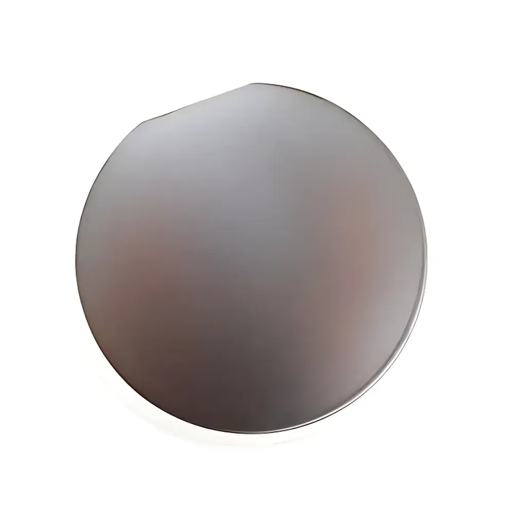
Si/SiO2/Ta/Cu Thin-Film Stack on Silicon Wafer
| Brand | 合肥科晶 |
|---|---|
| Origin | USA |
| Manufacturer Type | Authorized Distributor |
| Origin Category | Imported |
| Model | Si/SiO2/Ta/Cu Thin-Film Stack |
| Price | Upon Request |
| Cu Orientation | <111> |
| Cu Thickness | 100–400 nm (highly oriented polycrystalline) |
| Ta Thickness | 20–50 nm (diffusion barrier) |
| Si Substrate | <100> p-type, B-doped |
| SiO₂ Thickness | 300 nm |
| Si Resistivity | 1–20 Ω·cm |
| Wafer Diameter | 100 mm (4 inch) |
| Wafer Thickness | 525 µm |
| Surface Roughness | As-grown (≤0.3 nm RMS typical) |
| Packaging | Vacuum-sealed Class 100 clean bag in Class 1000 cleanroom or individual cassette |
Overview
The Si/SiO₂/Ta/Cu thin-film stack is a precisely engineered multilayer heterostructure designed for advanced microelectronics research, interconnect process development, and fundamental studies of copper electrodeposition, diffusion kinetics, and electromigration behavior. Fabricated on standard p-type boron-doped silicon wafers, the stack integrates a 300 nm thermally grown SiO₂ dielectric layer, a 20–50 nm sputtered tantalum adhesion/diffusion barrier, and a highly oriented polycrystalline copper top layer with strong texture—critical for low-resistivity interconnect performance and reliable electrochemical characterization. This architecture replicates key elements of back-end-of-line (BEOL) metallization schemes used in sub-65 nm CMOS technologies, enabling realistic evaluation of barrier integrity, Cu grain growth, and interfacial stability under thermal stress or electrical bias.
Key Features
- Highly oriented polycrystalline Cu layer (100–400 nm) with dominant crystallographic texture, confirmed by XRD and verified for enhanced conductivity and reduced surface scattering
- Ta diffusion barrier (20–50 nm) deposited via magnetron sputtering to suppress Cu–Si interdiffusion up to 400 °C, compliant with industry-standard thermal budget requirements
- Uniform 300 nm SiO₂ dielectric layer grown by dry oxidation—exhibiting low pinhole density, high breakdown field (>10 MV/cm), and stoichiometric consistency per ASTM F1570
- Single-side polished Si substrate (1–20 Ω·cm, boron-doped) with controlled carrier concentration and low dislocation density, suitable for transport measurements and device integration
- As-grown surface roughness ≤0.3 nm RMS (measured by AFM over 5×5 µm² area), minimizing nucleation variability during subsequent lithography or plating steps
- Available in two formats: full 100 mm (4-inch) wafers (525 µm thick) or diced 10×10 mm chips—both processed and packaged in ISO Class 4 (100) cleanroom environment
Sample Compatibility & Compliance
This thin-film stack is compatible with standard semiconductor metrology platforms including four-point probe resistivity mapping (ASTM F84), X-ray reflectivity (XRR), grazing-incidence XRD (GI-XRD), time-of-flight secondary ion mass spectrometry (ToF-SIMS), and transmission electron microscopy (TEM) cross-sectioning. All wafers undergo post-fabrication inspection per SEMI Standard M1–0309 for particle count and visual defects. Packaging adheres to SEMI E10–0206 specifications: vacuum-sealed in static-dissipative Class 100 clean bags within Class 1000 cleanroom conditions, with residual moisture content <5 ppm and O₂ <10 ppm. Traceability includes lot-specific certificates of conformance covering thickness uniformity (±3% across wafer), sheet resistance (reported as average ± standard deviation), and surface contamination screening (ICP-MS for Na, K, Fe, Ni, Cr).
Software & Data Management
While the film stack itself is a passive reference material, it is routinely integrated into automated test workflows using industry-standard data acquisition systems such as Keysight B1500A Semiconductor Parameter Analyzer or Keithley 4200-SCS. Measurement protocols are structured to comply with GLP and GMP documentation practices: all raw data files include embedded metadata (wafer ID, lot number, measurement date/time, operator ID, instrument calibration status). For traceable qualification in regulated environments (e.g., FDA-regulated R&D labs), the stack supports 21 CFR Part 11-compliant audit trails when used with validated software modules—enabling electronic signatures, version-controlled SOPs, and immutable data archiving.
Applications
- Calibration and validation of in-situ Cu electroplating monitoring tools (e.g., real-time optical reflectance, quartz crystal microbalance)
- Fundamental investigation of Ta/Cu interfacial reactions during rapid thermal annealing (RTA) and their impact on sheet resistance hysteresis
- Electromigration lifetime testing under constant current stress (CCS) per JEDEC JESD63 and IPC-TM-650 2.6.25
- Development and benchmarking of novel barrier materials (e.g., Co, Mn, Ru-based alloys) against Ta baseline performance
- Scanning probe microscopy (SPM) tip wear studies and nanoscale conductivity mapping using conductive-AFM
- Reference substrate for evaluating ALD/PVD tool chamber conditioning and cleaning efficacy
FAQ
Is this film stack suitable for direct use in photolithography processes?
Yes—surface planarity, low organic residue (<0.1 ng/cm² total carbon by XPS), and absence of metallic contaminants ensure compatibility with standard i-line and DUV photoresists.
Can I request custom Ta or Cu thicknesses outside the standard range?
Custom thicknesses (e.g., Ta = 10 nm or Cu = 800 nm) are available under NRE agreement; lead time increases by 4–6 weeks and requires minimum order quantity of 5 wafers.
Do you provide cross-sectional TEM samples prepared from these wafers?
No—TEM sample preparation (FIB lift-out, polishing, ion milling) must be performed by the end user or third-party service provider; however, we supply detailed handling guidelines to prevent interfacial delamination during sectioning.
What is the shelf life under recommended storage conditions?
When stored unopened at 20–25 °C and <30% RH in original packaging, the stack maintains interfacial integrity and surface oxide control for ≥12 months.
Are certificates of analysis (CoA) provided with each shipment?
Yes—each lot includes a CoA listing batch-specific XRF thickness verification, four-point probe sheet resistance maps (center, edge, corner), and SEMI-compliant particle count report.
 System")