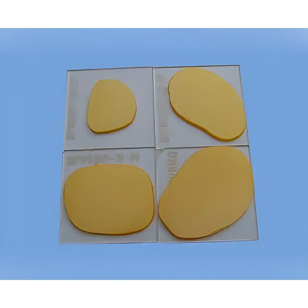
CdS Crystal Substrate (合肥科晶 | Model: CdS Crystal Substrate)
| Brand | Hefei Kejing |
|---|---|
| Origin | Anhui, China |
| Manufacturer Type | Authorized Distributor |
| Origin Category | Domestic (PRC) |
| Model | CdS Crystal Substrate |
| Price | Upon Request |
| Crystal Name | Cadmium Sulfide (CdS) |
| Growth Method | Physical Vapor Transport (PVT) |
| Crystal Structure | Hexagonal (Wurtzite) |
| Lattice Constants (Å) | a = 4.1367, c = 6.7161 |
| Density | 4.821 g/cm³ |
| Melting Point | 1287 °C |
| Specific Heat Capacity | 0.3814 J/g·K |
| Thermal Expansion Coefficient (×10⁻⁶/K) | 4.6 (∥a), 2.5 (∥c) |
| Thermal Conductivity (300 K) | 2.7 W/m·K |
| Transmission Range | 2.5–15 µm (>71% avg. transmittance) |
| Refractive Index | nₒ = 1.708, nₑ = 1.723 |
| Dimensions | 25 × 25 × 15 mm (custom orientations and dimensions available) |
Overview
CdS crystal substrates are single-crystal wafers of cadmium sulfide grown via physical vapor transport (PVT), engineered for high-performance optoelectronic and infrared (IR) applications. As a II–VI compound semiconductor, CdS exhibits a direct bandgap (~2.42 eV at 300 K), enabling efficient photon absorption and emission in the visible to near-IR spectrum. Its hexagonal wurtzite structure provides intrinsic birefringence and strong anisotropic optical properties—critical for polarization-sensitive devices, nonlinear frequency conversion, and IR window or lens substrates operating beyond 2.5 µm. With broad spectral transparency from 2.5 µm to 15 µm (average transmission >71%), low thermal expansion along the c-axis (2.5 × 10⁻⁶/K), and moderate thermal conductivity (2.7 W/m·K at 300 K), CdS substrates serve as stable mechanical and optical platforms for thin-film epitaxy, photoconductive detectors, and mid-IR optical components.
Key Features
- High-purity single-crystal CdS grown by controlled PVT method, minimizing point defects and dislocation density
- Hexagonal wurtzite lattice with precisely characterized lattice parameters (a = 4.1367 Å, c = 6.7161 Å) for predictable epitaxial strain matching
- Anisotropic thermal expansion coefficients (4.6 × 10⁻⁶/K ∥ a-axis; 2.5 × 10⁻⁶/K ∥ c-axis) supporting thermally stable mounting in cryogenic or high-flux optical systems
- Optical-grade surface finish suitable for subsequent thin-film deposition (e.g., ALD, sputtering, MBE) without polishing-induced subsurface damage
- Customizable crystallographic orientation (e.g., (0001), (101̅0), (112̅0)) and dimensional tolerances (±0.1 mm on length/width, ±0.05 mm on thickness)
- Handled and packaged in ISO Class 1000 cleanroom environment; individual substrates sealed in ISO Class 100 clean bags or static-dissipative single-wafer carriers
Sample Compatibility & Compliance
CdS substrates are compatible with standard semiconductor fabrication protocols including photolithography, reactive ion etching (RIE), and metalorganic chemical vapor deposition (MOCVD). Their wide bandgap and chemical stability support integration into heterostructures with ZnS, ZnSe, or GaP layers. While CdS is not RoHS-exempt due to cadmium content, it complies with IEC 62321-7-2 for restricted substance screening when used in research-grade instrumentation under controlled handling. Substrates meet ASTM F1529-19 requirements for crystalline semiconductor wafer flatness and surface particulate limits (<10 particles ≥0.5 µm per cm²). For regulated end-use (e.g., medical IR sensors), full material traceability—including growth batch ID, XRD rocking curve FWHM data, and FTIR transmission spectra—is provided upon request.
Software & Data Management
No embedded firmware or proprietary software is associated with bare CdS crystal substrates. However, substrate specifications are fully compatible with industry-standard metrology workflows: surface topography data (from AFM or white-light interferometry) may be imported into Bruker NanoScope Analysis or Zygo MetroPro; optical transmission spectra align with Ocean Insight OceanView or Thermo Fisher OMNIC calibration libraries; and crystallographic orientation reports integrate with Rigaku SmartLab or PANalytical Empyrean diffraction analysis suites. All supplied documentation—including certificate of conformance, XRD pole figure maps, and spectral transmission reports—is delivered in PDF/A-1b format for long-term archival compliance with ISO 15489-1 and FDA 21 CFR Part 11 record-keeping standards.
Applications
- Substrate for epitaxial growth of CdTe, ZnTe, or HgCdTe infrared detector heterostructures
- Active element in photoconductive switches and visible-light photodetectors
- Nonlinear optical component for second-harmonic generation (SHG) in tunable OPO systems (phase-matching achievable at specific angles due to birefringence)
- Transmissive window or beam splitter in Fourier-transform infrared (FTIR) spectrometers operating between 2.5–12 µm
- Calibration reference for IR radiometry and blackbody source characterization
- Research platform for studying excitonic effects, defect luminescence, and carrier recombination dynamics in wide-bandgap semiconductors
FAQ
Is this CdS substrate suitable for high-vacuum or UHV deposition environments?
Yes—substrates undergo solvent-free plasma cleaning prior to packaging and exhibit negligible outgassing rates (<1 × 10⁻¹⁰ Torr·L/s·cm²) after 24 h bakeout at 150 °C, meeting UHV compatibility thresholds per ASTM E1557.
Can you provide substrates with (0001) orientation and off-cut?
Yes—standard offerings include c-plane (0001) orientation with optional 0.5° or 2.0° off-cut toward m-plane; off-cut angle tolerance is ±0.1°, verified by high-resolution XRD ω-scan.
What surface finish options are available?
Standard finish is mechanical polish (Ra < 0.5 nm); chemical-mechanical polish (Ra < 0.2 nm) and epitaxial-ready etch (for atomically terraced surfaces) are available as value-added services with lead-time extension.
Do you supply substrates with pre-deposited AR coatings?
No—AR coatings are not offered as standard; however, we provide coating design files (TFCalc-compatible) optimized for 3–12 µm broadband antireflection on CdS, along with recommended deposition parameters for e-beam evaporation.
Is MSDS documentation available for CdS substrates?
Yes—a full SDS compliant with GHS Rev. 10 and CLP Regulation (EC) No. 1272/2008 is issued for each shipment, including hazard statements (H350i, H373), safe handling instructions, and disposal guidance per local environmental regulations.


 System")
