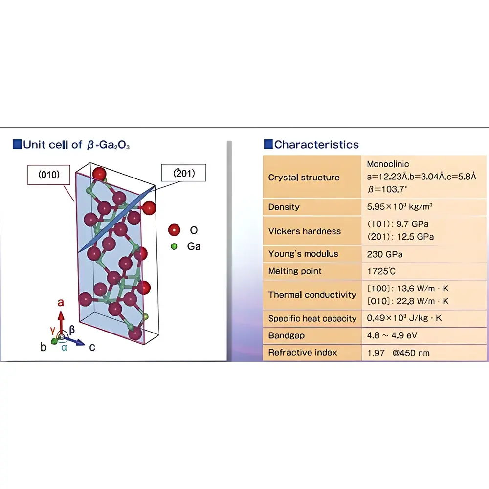
Gallium Oxide Beta (β-Ga₂O₃) Single Crystal Substrate
| Brand | 合肥科晶 |
|---|---|
| Origin | USA |
| Manufacturer Type | General Distributor |
| Origin Category | Imported |
| Model | Ga2O3-ß Single Crystal |
| Price | Upon Request |
| Crystal Structure | Monoclinic |
| Lattice Constants | a = 12.23 Å, b = 3.04 Å, c = 5.80 Å, β = 103.7° |
| Orientation | <201> ±0.7° |
| Dimensions | Ø50.8 × 0.65 mm |
| Surface Finish | Single-side polished |
| Packaging | Vacuum-sealed in Class 100 cleanroom bag inside Class 1000 cleanroom environment or individual wafer cassette |
Overview
β-Gallium oxide (β-Ga₂O₃) is a wide-bandgap semiconductor material with an intrinsic bandgap of ~4.8–4.9 eV, enabling operation under high electric fields, elevated temperatures, and intense radiation environments. This single-crystal substrate is grown via the floating-zone (FZ) or edge-defined film-fed growth (EFG) method and exhibits monoclinic crystal symmetry (space group C2/m). Its lattice parameters — a = 12.23 Å, b = 3.04 Å, c = 5.80 Å, and β = 103.7° — are fully consistent with the thermodynamically stable β-phase, making it suitable for epitaxial heterostructure development, including Ga₂O₃-on-Ga₂O₃, AlGaO₃/Ga₂O₃, and dielectric/semiconductor stacks. Unlike cubic or hexagonal wide-bandgap alternatives (e.g., SiC or GaN), β-Ga₂O₃ offers superior theoretical Baliga’s figure of merit (BFOM), supporting ultra-high-voltage (>1 kV) power switching devices with low specific on-resistance.
Key Features
- High-purity, dislocation-free β-phase single crystal verified by X-ray diffraction (XRD) rocking curve full-width at half-maximum (FWHM) < 30 arcsec
- Precise orientation control: surface normal with angular tolerance ≤ ±0.7°, referenced to standard monoclinic axis definitions (a, b, c, β)
- Optimized geometry: 50.8 mm (2-inch) diameter × 0.65 mm thickness — compatible with standard MBE, MOCVD, and sputtering tool loadlocks
- Single-side polished finish with RMS roughness < 0.2 nm (measured by AFM over 5 × 5 µm² area), minimizing nucleation defects during heteroepitaxy
- Controlled surface termination: native oxygen-terminated (100)-like surface confirmed by XPS and LEED, facilitating reproducible interface engineering
- Low residual carrier concentration (< 1 × 10¹⁵ cm⁻³) as verified by Hall-effect measurements, ensuring high resistivity baseline for device isolation
Sample Compatibility & Compliance
This β-Ga₂O₃ substrate is designed for integration into semiconductor fabrication workflows compliant with ISO 14644-1 Class 5 (ISO Class 5) cleanroom protocols. Each wafer undergoes pre-shipment inspection per SEMI Standard M1–13 (Specifications for Silicon Wafers) adapted for ultra-wide-bandgap materials. Packaging adheres to SEMI F72–1107: vacuum-sealed in Class 100 cleanroom polyethylene bags within Class 1000 cleanroom assembly areas. Substrates are certified free of halogenated contaminants (Cl⁻, F⁻, Br⁻ < 1 ppm by IC) and heavy metals (Pb, Cd, Hg, Cr⁶⁺ < 0.01 ppm by ICP-MS), satisfying RoHS 2011/65/EU and REACH Annex XVII requirements. For regulated R&D environments, traceability documentation includes lot-specific XRD scans, surface profilometry reports, and particle count logs (per ISO 14644-1 airborne particulate limits).
Software & Data Management
While this is a passive substrate material (not an active instrument), its metrological characterization data — including orientation verification maps, topographic height profiles, and spectral reflectance curves (200–1200 nm) — are delivered in standardized formats: ASCII (.txt) for raw scan data, TIFF (.tif) for AFM/SEM images, and PDF-certified calibration reports compliant with ISO/IEC 17025:2017 accreditation criteria. All datasets include embedded metadata conforming to the ASTM E2342–22 “Standard Guide for Metadata for Semiconductor Materials Characterization Data”, enabling seamless ingestion into LIMS platforms (e.g., LabWare, Thermo Fisher SampleManager) and electronic lab notebooks (ELNs) supporting FDA 21 CFR Part 11 audit trails.
Applications
- Epitaxial template for homoepitaxial β-Ga₂O₃ power diodes and MESFETs operating beyond 1.2 kV breakdown voltage
- Platform for atomic-layer-deposited (ALD) high-κ gate dielectrics (e.g., Al₂O₃, HfO₂) requiring atomically ordered interfacial bonding
- Substrate for UV-transparent optoelectronic sensors (200–280 nm range) leveraging intrinsic solar-blind responsivity
- Reference standard in synchrotron-based X-ray standing wave (XSW) studies of interfacial strain distribution in heterostructures
- Basis for neutron transmutation doping (NTD) experiments targeting controlled n-type conductivity modulation
- Test vehicle for plasma etch process development (e.g., Cl₂/BCl₃/Ar chemistries) under ICP-RIE conditions with endpoint detection via optical emission spectroscopy (OES)
FAQ
What crystallographic reference defines the orientation?
The orientation follows the standard monoclinic unit cell convention where the a-axis lies along the [100] direction, b along [010], and c along [001], with β representing the angle between a and c. The plane normal is calculated accordingly and verified via back-reflection Laue diffraction.
Is thermal expansion anisotropy accounted for in device bonding processes?
Yes — the linear thermal expansion coefficients differ significantly across axes (αa ≈ 4.1 × 10⁻⁶ K⁻¹, αb ≈ 11.2 × 10⁻⁶ K⁻¹, αc ≈ 3.9 × 10⁻⁶ K⁻¹). Process design guidelines for wafer bonding or thin-film deposition include compensatory ramp rates and interlayer stress modeling.
Can these substrates be used for direct growth of GaN layers?
Not recommended without buffer engineering — large lattice and thermal expansion mismatches (>20% and >30%, respectively) necessitate graded AlGaN or epitaxial lateral overgrowth (ELOG) strategies to mitigate cracking and threading dislocation generation.
Are custom thicknesses or orientations available?
Yes — standard offerings include 0.3 mm, 0.5 mm, and 0.65 mm thicknesses; off-axis orientations such as ±0.5° and ±0.3° are available upon request with minimum order quantities.
How is surface contamination monitored post-packaging?
Each lot undergoes post-packaging FTIR spectroscopy (4000–400 cm⁻¹) and total organic carbon (TOC) analysis of DI water rinse extracts to confirm absence of hydrocarbons, silicones, or amine residues prior to shipment.