MgO Crystal Substrate (KJ-MgO Series) by Hefei Kejing
| Brand | Hefei Kejing |
|---|---|
| Origin | Anhui, China |
| Manufacturer Type | Authorized Distributor |
| Origin Category | Domestic |
| Model | MgO Crystal Substrate |
| Price | Upon Request |
| Crystal Structure | Cubic |
| Lattice Constant | a = 4.216 Å |
| Growth Method | Arc Melting |
| Melting Point | 2850 °C |
| Density | 3.58 g/cm³ |
| Mohs Hardness | 5.5 |
| Thermal Expansion Coefficient | 12.8 × 10⁻⁶ /°C |
| Dielectric Constant | 9.8 |
| Optical Transmittance | >90% @ 200–400 nm, >98% @ 500–1000 nm |
| Cleavage Plane | <100> |
| Orientations Available | <100>, <110>, <111> |
| Orientation Tolerance | ±0.5° |
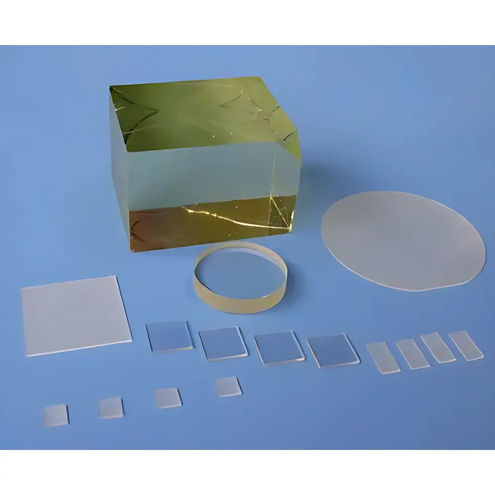
| Standard Dimensions | Ø2" × 0.5 mm, 10 × 10 × 0.5 mm, 10 × 5 × 0.5 mm |
| Surface Finish | Single- or Double-Polished |
| Surface Roughness | Ra <15 Å for <111>, Ra <5 Å for <100> and <110> |
| Packaging | Class 1000 Cleanroom, Class 100 Clean Bag or Individual Wafer Cassette |
Overview
The MgO Crystal Substrate (KJ-MgO Series) is a high-purity, single-crystal magnesium oxide substrate engineered for epitaxial thin-film deposition in advanced functional materials research and industrial device fabrication. As a cubic periclase-structured oxide with lattice parameter a = 4.216 Å, MgO offers exceptional structural compatibility with numerous perovskite, spinel, and layered oxide systems—including high-temperature superconductors (e.g., YBCO), ferroelectrics (e.g., PZT, SBT), magnetic oxides (e.g., LSMO, LCMO), and wide-bandgap optoelectronic materials. Its low dielectric loss (tan δ < 10⁻⁴) and stable permittivity (εr ≈ 9.8) across microwave frequencies make it a preferred platform for RF/microwave filters, resonators, and integrated passive devices in 5G and satellite communication systems. Grown via controlled arc melting—a technique enabling high stoichiometric fidelity and minimized point defects—the KJ-MgO substrates are processed under ISO Class 5 (Class 100) cleanroom conditions and finished using chemical-mechanical polishing (CMP) to achieve atomically flat surfaces essential for monolayer-controlled growth.
Key Features
- High-purity single crystal grown by optimized arc melting, minimizing oxygen vacancies and metallic impurities
- Atomically smooth surface finish: Ra < 5 Å for and orientations; Ra < 15 Å for orientation
- Low thermal expansion mismatch with common functional oxides (e.g., Δα/α < 2% vs. YBCO at 77 K)
- Wide optical transparency from deep UV (200 nm) to near-IR (1000 nm), supporting in situ spectroscopic monitoring during deposition
- Available in standard wafer formats (Ø2″ × 0.5 mm) and custom rectangular geometries (e.g., 10 × 10 × 0.5 mm, 10 × 5 × 0.5 mm)
- Orientation tolerance strictly controlled to ±0.5°, certified via high-resolution X-ray diffraction (HR-XRD) rocking curve analysis
- Double-polished options include front-side CMP and back-side lapping for enhanced parallelism (<5 arcsec total thickness variation)
Sample Compatibility & Compliance
KJ-MgO substrates are routinely used in pulsed laser deposition (PLD), sputtering, molecular beam epitaxy (MBE), and metalorganic chemical vapor deposition (MOCVD) systems. Their chemical inertness above 800 °C and resistance to halogen-based etchants ensure compatibility with aggressive thin-film processing chemistries. All substrates undergo rigorous metrological validation per ASTM F1726-20 (Standard Practice for Specification of Silicon Wafers) adapted for oxide crystals—covering surface particulate count (per SEM/EDS), residual metal contamination (<1 × 10¹⁰ atoms/cm² for Fe, Ni, Cr), and crystalline defect density (<5 × 10³ cm⁻² etch pit density). Packaging complies with SEMI F72-1102 (Cleanroom Packaging for Semiconductor Wafers) and supports GLP-compliant traceability through batch-specific QC reports including XRD θ–2θ scans and AFM topography maps.
Software & Data Management
While the MgO substrate itself is a passive material platform, its integration into automated thin-film manufacturing workflows requires full traceability. Each substrate lot is assigned a unique alphanumeric identifier linked to a secure digital QC dossier containing: (i) orientation verification report (XRD pole figure + rocking curve FWHM), (ii) surface roughness map (AFM scan area ≥ 5 × 5 µm²), (iii) optical transmission spectrum (200–1000 nm, 1 nm resolution), and (iv) cleanliness certification (particle count per ISO 14644-1 Class 5). These datasets are provided in vendor-neutral CSV and PDF formats compatible with laboratory information management systems (LIMS) and comply with FDA 21 CFR Part 11 requirements for electronic records and signatures when deployed in regulated R&D environments.
Applications
- Epitaxial growth of YBa₂Cu₃O7−δ (YBCO) and Tl-based high-Tc superconducting films for microwave bandpass filters and kinetic inductance detectors (KIDs)
- Template layers for strain-engineered ferroelectric heterostructures (e.g., BaTiO₃ on MgO for negative capacitance transistors)
- Substrates for spintronic oxide interfaces (e.g., La₀.₇Sr₀.₃MnO₃/MgO/Fe tunnel junctions)
- Platform for ultrathin dielectric gate stacks in wide-bandgap semiconductor devices (e.g., GaN-on-MgO)
- Reference standards in X-ray reflectivity (XRR) and grazing-incidence small-angle X-ray scattering (GISAXS) calibration
- UV-transparent windows and beam splitters in synchrotron and ultrafast laser optics
FAQ
What is the maximum operating temperature for MgO substrates in vacuum deposition systems?
MgO retains structural integrity up to 1200 °C in high-vacuum (<10⁻⁶ Torr) or O₂ ambient; prolonged exposure above 1300 °C may induce surface decomposition or step-bunching.
Can MgO substrates be cleaned using RCA protocols?
Yes—standard SC-1 (NH₄OH:H₂O₂:H₂O) and SC-2 (HCl:H₂O₂:H₂O) treatments are effective; however, HF-based etches must be avoided due to MgF₂ formation and surface pitting.
Do you provide orientation-certified substrates with full XRD characterization data?
Yes—every shipment includes a certificate of analysis with θ–2θ scan, rocking curve FWHM, and pole figure data acquired on a Bruker D8 Discover diffractometer.
Are double-polished MgO wafers suitable for optical interferometry applications?
Yes—double-polished wafers with parallelism <5 arcsec and surface flatness λ/10 @ 633 nm meet ISO 10110-7 specifications for precision optical substrates.
Is custom cutting and edge profiling available?
Yes—custom geometries, chamfered edges (0.1–0.3 mm radius), and laser-scribed alignment notches (per SEMI MF1530) can be accommodated upon request with NDA-compliant documentation.