CaF2 Crystal Substrates –合肥科晶 (Hefei Kejing) High-Purity Calcium Fluoride Optical Windows & Substrates
| Brand | Hefei Kejing |
|---|---|
| Origin | Anhui, China |
| Manufacturer Type | Authorized Distributor |
| Country of Origin | PRC |
| Model | CaF₂ Crystal Substrate |
| Price | Upon Request |
| Crystal Structure | Cubic |
| Lattice Constant | 5.462 Å |
| Melting Point | 1418 °C |
| Density | 3.18 g/cm³ |
| Mohs Hardness | 4 |
| Thermal Expansion Coefficient | 18.85 × 10⁻⁶ /°C |
| Refractive Index (at 5 µm) | 1.43382 |
| Transmission Range | 0.11–12.0 µm |
| Transmission | >94% @ 5 µm, >85% @ 0.2 µm |
| Abbe Number (νd) | 0.00455 |
| dn/dT @ 0.8 µm | −10.6 × 10⁻⁶ /°C |
| Growth Method | Bridgman |
| Standard Orientations | <100>, <111> |
| Standard Dimensions | 5×5×0.5 mm, 10×10×0.5 mm, Ø25.4×0.5 mm, Ø101.6×0.5 mm |
| Surface Finish | Single-side or Double-side Polished |
| Surface Roughness (Ra) | <5 Å |
| Packaging | Class 1000 Cleanroom Assembly, Class 100 Clean Bag or Individual Protective Cassette |
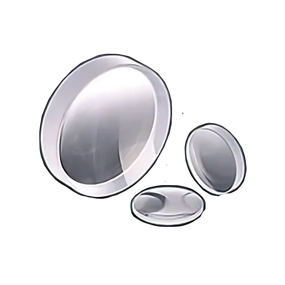
Overview
CaF2 crystal substrates from Hefei Kejing are high-purity, optically homogeneous calcium fluoride wafers engineered for demanding ultraviolet (UV), visible (VIS), and mid-infrared (MIR) optical applications. As a cubic ionic crystal grown via the vertical Bridgman method, CaF2 exhibits exceptional transmission from 110 nm to 12 µm—spanning deep UV through thermal IR—with minimal absorption and low birefringence. Its isotropic nature, combined with a low refractive index (n ≈ 1.43 at 5 µm) and negligible dispersion in the MIR, makes it ideal for broadband windows, beam splitters, prisms, laser cavity optics, and spectroscopic substrates where phase stability and spectral fidelity are critical. Unlike fused silica or sapphire, CaF2 maintains high transmission below 190 nm—enabling use in excimer laser systems (e.g., ArF at 193 nm, F2 at 157 nm) and synchrotron beamlines requiring VUV transparency.
Key Features
- Ultra-broadband transmission: 0.11–12.0 µm with >94% absolute transmittance at 5 µm and >85% at 200 nm (uncoated, 0.5 mm thickness)
- Precision crystallographic orientation: Standard and cuts available; custom orientations (e.g., , off-axis) supported per ASTM F1727-22 specifications
- Atomic-level surface quality: Ra < 0.5 nm (<5 Å) on single- or double-side polished faces, compliant with ISO 10110-7 surface roughness standards
- Thermally stable architecture: Low dn/dT (−10.6 × 10⁻⁶/°C at 0.8 µm) and moderate thermal expansion (18.85 × 10⁻⁶/°C) enable stable performance across laboratory and industrial environmental gradients
- Controlled defect density: Grown under inert atmosphere with post-growth annealing to minimize color centers and scattering inclusions—verified by laser scatter inspection per MIL-PRF-13830B
- Class 100 cleanroom handling: Packaged in ISO Class 5 (100) clean bags or individual protective cassettes within ISO Class 6 (1000) assembly environment
Sample Compatibility & Compliance
Hefei Kejing CaF2 substrates are compatible with standard thin-film deposition processes—including electron-beam evaporation, ion-assisted deposition (IAD), and atomic layer deposition (ALD)—without interfacial delamination or substrate-induced stress cracking. The material’s low chemical reactivity and resistance to non-aqueous etchants (e.g., HF-free cleaning chemistries) support integration into semiconductor metrology, photolithography mask blanks, and cryogenic detector assemblies. All batches undergo full traceability documentation aligned with ISO 9001:2015 manufacturing controls. Certificates of Conformance include lattice parameter verification (XRD), residual stress mapping (Raman microspectroscopy), and spectral transmission validation per ISO 9050:2022 Annex D protocols. Optional GLP-compliant test reports (including spectral scans from 110 nm to 12 µm) are available upon request.
Software & Data Management
While CaF2 substrates are passive optical components, Hefei Kejing provides digital material dossiers for each batch, including spectral transmission curves (measured on PerkinElmer Lambda 1050+ with integrating sphere and deuterium/Xe lamp sources), surface topography maps (via Veeco Wyko NT1100 interferometry), and crystallographic orientation confirmation (Oriented X-ray Diffraction). These datasets are delivered in standardized CSV and PDF formats, compatible with LIMS environments and compliant with FDA 21 CFR Part 11 requirements when paired with electronic signature-enabled delivery platforms. Custom spectral modeling (e.g., Sellmeier coefficient fitting, multi-angle reflectance simulation) is supported via MATLAB- or Python-based optical design toolkits (Zemax OpticStudio, CODE V, ASAP).
Applications
- Deep-UV lithography optics and excimer laser windows (ArF, KrF, F2)
- Infrared spectroscopy cells, FTIR beam combiners, and QCL output couplers
- Cryogenic detector substrates for astronomical instrumentation (e.g., JWST NIRSpec calibration elements)
- Reference standards for radiometric calibration in NIST-traceable UV-VIS-NIR spectrophotometers
- Substrates for epitaxial growth of II-VI and III-V semiconductors (e.g., CdTe, HgCdTe) due to lattice matching and thermal expansion compatibility
- Plasma-facing components in fusion diagnostics requiring high-Z impurity resistance and low neutron activation
FAQ
What is the typical wavefront distortion for a 10×10×0.5 mm CaF2 substrate polished to λ/10 at 633 nm?
Standard double-side polished substrates meet λ/4 PV wavefront error (WFE) over aperture; λ/10 WFE is achievable with optional precision figure correction and is documented in the Certificate of Conformance.
Can these substrates be used in ultra-high vacuum (UHV) environments?
Yes—CaF2 exhibits low outgassing rates (<1×10⁻¹⁰ Torr·L/s·cm² after 24-h bakeout at 120°C) and is compatible with UHV-compatible cleaning protocols (e.g., oxygen plasma followed by methanol/IPA rinse).
Is coating adhesion tested per MIL-C-48497A?
Coating adhesion qualification (tape test, scratch test per ASTM D3359 and ISO 2409) is performed on coated samples; uncoated substrates are supplied with verified surface energy (>42 mN/m) and hydrophilicity (contact angle <10°) to ensure robust film nucleation.
Do you provide orientation verification via Laue diffraction?
Yes—each lot includes Laue back-reflection patterns and orientation deviation reports referenced to NIST SRM 1977 Si standard.