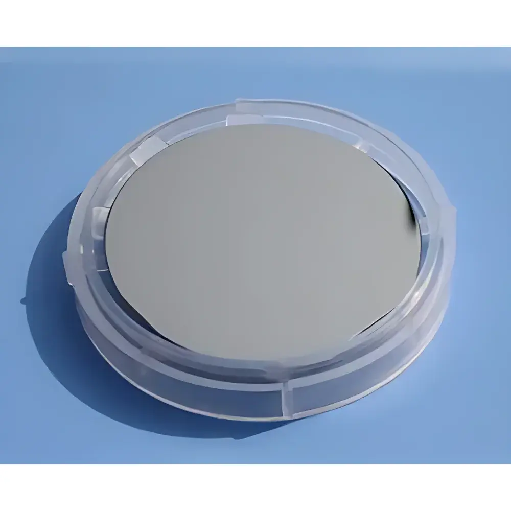
InSb (Indium Antimonide) Single Crystal Wafers – P-type Ge-doped, LEC-Grown, Orientation
| Brand | Hefei Kejing |
|---|---|
| Origin | USA |
| Manufacturer Type | Authorized Distributor |
| Origin Category | Imported |
| Model | InSb (Imported) |
| Pricing | Available Upon Request |
Overview
InSb (Indium Antimonide) single crystal wafers are critical semiconductor substrates widely employed in mid- to long-wave infrared (MWIR–LWIR, 3–12 µm) photodetectors, Hall sensors, magnetoresistive devices, and cryogenic quantum transport studies. This product line consists of high-purity, p-type germanium-doped InSb wafers grown via the Liquid Encapsulated Czochralski (LEC) method—a standard industrial technique for producing low-defect, stoichiometric III–V compound semiconductors under controlled phosphorus or boron oxide encapsulation. The crystallographic orientation (±0.5° tolerance) ensures optimal epitaxial compatibility with common IR detector architectures, including photoconductive and photovoltaic heterostructures. With carrier concentrations tunable between 0.05–0.50 × 1017 cm−3 and electron mobilities exceeding 4.0–8.4 × 103 cm2/V·s at room temperature, these wafers support high-sensitivity, low-noise device fabrication under both ambient and cryogenic operating conditions.
Key Features
- High-purity, p-type InSb substrate doped with germanium—engineered for stable acceptor activation and uniform dopant distribution
- LEC growth process ensures low dislocation density: etch pit density (EPD) < 200 cm−2, verified by standard molten KOH etching per ASTM F1722
- Precise crystallographic orientation (±0.5°), certified via X-ray diffraction rocking curve analysis (θ–2θ scan)
- Standard geometry: 50.8 mm (2 inch) diameter × 0.45 mm thickness, with single-side mechanical polish achieving surface roughness < 5 Å RMS (measured by AFM)
- Controlled carrier concentration range: 5 × 10¹⁶–5 × 1017 cm−3, enabling optimization for either high-responsivity photodetection or low-offset Hall sensing
- Processed and packaged in ISO Class 4 (100-level) cleanroom environment; individually sealed in vacuum-packed, static-dissipative 100-class clean bags or rigid wafer cassettes
Sample Compatibility & Compliance
These InSb wafers are compatible with standard III–V semiconductor processing workflows, including thermal evaporation, sputtering, photolithography (i-line and g-line), wet/dry etching (e.g., HCl:H3PO4:H2O), and dielectric passivation (e.g., SiO2, SiNx). All wafers undergo full electrical characterization—including Van der Pauw resistivity and Hall effect measurements per ASTM F76—prior to shipment. Certificates of Conformance (CoC) include batch-specific EPD maps, orientation verification reports, and carrier mobility data. Packaging complies with JEDEC J-STD-033 for moisture sensitivity level (MSL) 1 handling, and materials documentation conforms to RoHS Directive 2011/65/EU and REACH Regulation (EC) No. 1907/2006.
Software & Data Management
While the InSb wafers themselves are passive substrates, their metrological traceability is supported through integrated quality management systems compliant with ISO 9001:2015. Batch-level test data—including EPD histograms, XRD full-width-at-half-maximum (FWHM) values, and four-point probe sheet resistance maps—are archived in secure, audit-ready formats. For customers requiring extended traceability in regulated environments (e.g., defense IR systems or medical imaging R&D), optional GLP-aligned documentation packages—including raw measurement logs, equipment calibration certificates (NIST-traceable), and analyst sign-offs—are available upon request. All data files are delivered in CSV and PDF formats, compatible with LIMS integration.
Applications
- Front-side illuminated MWIR photodiodes and focal plane arrays (FPAs) for thermal imaging and spectroscopy
- Low-field Hall sensors used in automotive current monitoring, precision current clamps, and magnetic field mapping systems
- Substrates for molecular beam epitaxy (MBE) and metalorganic chemical vapor deposition (MOCVD) of InSb-based heterostructures (e.g., InAs/InSb superlattices)
- Cryogenic quantum Hall effect and Shubnikov–de Haas oscillation studies below 4 K
- Reference standards in infrared optical testing, particularly for calibrating spectral responsivity of FTIR detectors
- Research platforms for topological insulator interface engineering and 2D electron gas (2DEG) confinement studies
FAQ
What is the typical lead time for custom-dimension or alternate-doping InSb wafers?
Standard 2-inch, 0.45-mm-thick, Ge-doped wafers ship within 5–7 business days from order confirmation. Custom specifications—including alternative orientations (, ), thicknesses (0.3–1.0 mm), double-side polish, or Sn/Si doping—require a minimum 6–8 week production cycle due to LEC crystal growth scheduling.
Do you provide epitaxial-ready surfaces or native oxide removal services?
Yes. Optional NH4OH/H2O2/H2O (SC-1) cleaning and in-situ oxide desorption via ultra-high-vacuum (UHV) annealing (≤450 °C, 10−9 Torr) are available as value-added services. Surface preparation reports include XPS O 1s peak analysis and contact angle measurements.
Is material certification available for export-controlled applications (e.g., ITAR/EAR99)?
All InSb wafers are classified EAR99 and shipped with dual-use commodity classification rulings. ITAR-free documentation packages—including non-proprietary crystal growth parameters and non-sensitive defect metrics—are provided upon validated end-user statement submission.