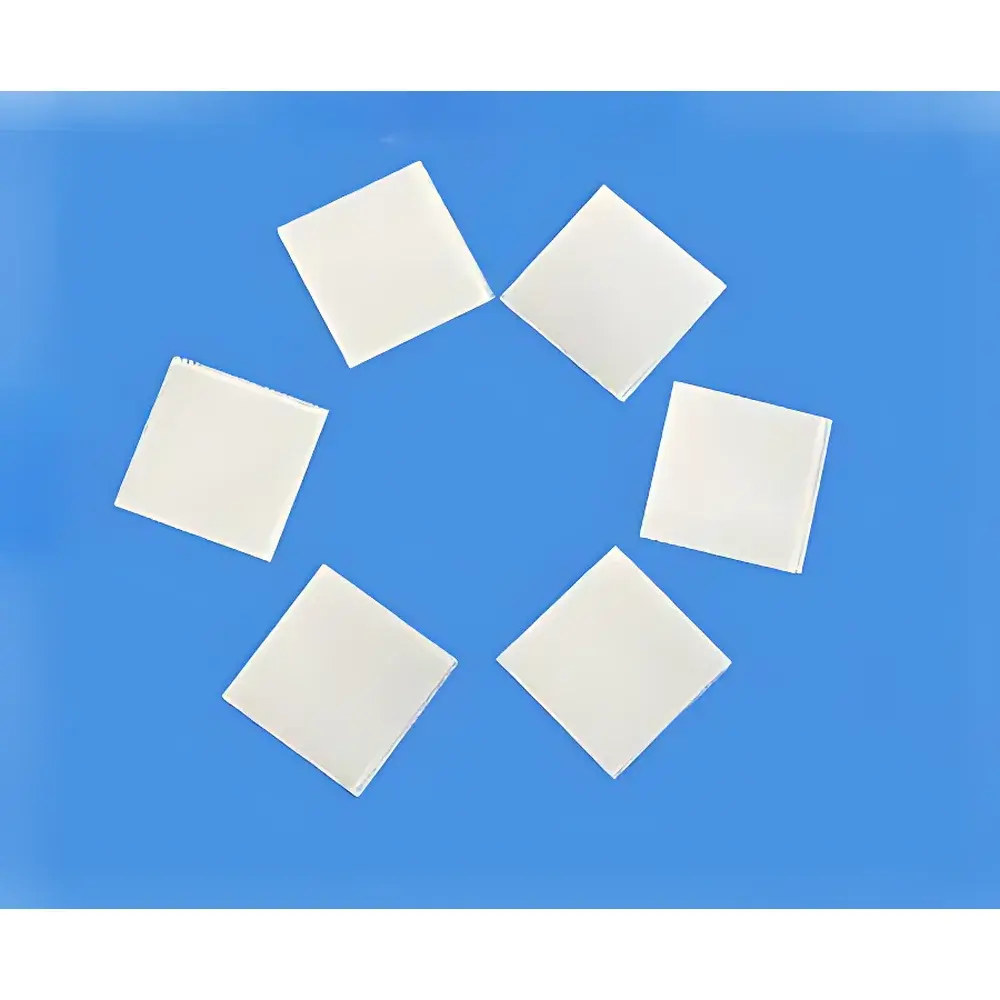
LiAlO₂ Lithium Aluminate Single-Crystal Substrates
| Brand | Hefei Kejing |
|---|---|
| Origin | Anhui, China |
| Manufacturer Type | Authorized Distributor |
| Origin Category | Domestic |
| Model | LiAlO₂ |
| Pricing | Available Upon Request |
| Crystal Structure | Tetragonal |
| Lattice Constants | a = 5.17 Å, c = 6.26 Å |
| Lattice Mismatch with GaN (001) | 1.4% |
| Melting Point | 1900 °C |
| Density | 2.62 g/cm³ |
| Mohs Hardness | 7.5 |
| Standard Orientations | <100>, <001> |
| Orientation Tolerance | ±0.5° |
| Standard Dimensions | Ø2" × 0.5 mm, 10 × 10 × 0.5 mm, 10 × 5 × 0.5 mm, 5 × 5 × 0.5 mm |
| Surface Finish | Fine-ground, Single-side Polished, or Double-side Polished |
| Packaging | Class 1000 Cleanroom Fabrication, Sealed in Class 100 Clean Bags |
Overview
Lithium aluminate (LiAlO₂) single-crystal substrates are engineered for high-precision epitaxial growth of wide-bandgap semiconductor thin films—particularly gallium nitride (GaN) and related III-nitride compounds. Their tetragonal crystal structure (space group I41/amd) exhibits exceptional lattice compatibility with GaN along the (001) plane, with a measured mismatch of only 1.4%. This low interfacial strain enables reduced threading dislocation density, improved crystalline coherence, and enhanced device performance in high-electron-mobility transistors (HEMTs), UV LEDs, and laser diodes. With a high melting point of 1900 °C and thermal stability up to 1200 °C in inert or reducing atmospheres, LiAlO₂ substrates maintain structural integrity during metalorganic chemical vapor deposition (MOCVD) and molecular beam epitaxy (MBE) processes. Its moderate density (2.62 g/cm³) and Mohs hardness of 7.5 ensure mechanical robustness during wafer handling, polishing, and thin-film sputtering without excessive chipping or subsurface damage.
Key Features
- Tetragonal single-crystal structure optimized for heteroepitaxial GaN growth with minimal interfacial strain
- Precisely controlled orientation tolerances (±0.5°) for reproducible epitaxial alignment
- Available in standard orientations: and , with custom off-axis cuts available upon request
- Multiple thickness options (0.5 mm standard) compatible with standard vacuum chucking and RF sputtering fixtures
- Surface finish options include fine-ground, single-side polished (SSP), and double-side polished (DSP) configurations—each certified via atomic force microscopy (AFM) and optical interferometry
- Class 1000 cleanroom fabrication and Class 100 clean-bag packaging ensure particulate contamination <10 particles/m³ (≥0.5 µm)
Sample Compatibility & Compliance
LiAlO₂ substrates are chemically inert under typical MOCVD precursor environments (e.g., NH₃, TMGa, TMAI) and exhibit negligible interdiffusion with GaN layers up to 1000 °C. They are compatible with standard quartz boat loading, resistive heating stages, and plasma-assisted deposition systems. All wafers undergo post-processing inspection per SEMI MF1390 and ISO 14644-1 standards. Certificate of Conformance includes X-ray diffraction (XRD) rocking curve full-width at half-maximum (FWHM) data, surface roughness (Ra < 0.3 nm for DSP), and orientation verification via Laue back-reflection. Documentation supports GLP-compliant thin-film R&D workflows and is traceable to NIST-traceable calibration references.
Software & Data Management
While LiAlO₂ substrates are passive components, their integration into automated thin-film platforms—including QCM-based in-situ monitoring systems—requires precise substrate metadata management. Each batch is assigned a unique Lot ID linked to QC reports accessible via secure web portal (username/password authenticated). Digital records include XRD spectra, AFM topography maps, and optical flatness measurements (Zygo Verifire™ Interferometer). For users operating under FDA 21 CFR Part 11 or EU Annex 11 requirements, audit trails for lot release, packaging validation, and environmental monitoring logs are retained for ≥10 years.
Applications
- Heteroepitaxial GaN-on-LiAlO₂ for high-frequency power electronics and RF amplifiers
- Template layer for subsequent growth of AlN buffer layers in deep-UV optoelectronics
- Substrate for lithium-ion battery cathode material studies using in-situ XRD and electrochemical impedance spectroscopy (EIS)
- Platform for solid-state electrolyte interface characterization in all-solid-state battery research
- Reference substrate in quartz crystal microbalance (QCM) sensor development for gas-phase adsorption kinetics
- Calibration standard for lattice parameter benchmarking in synchrotron-based diffraction experiments
FAQ
What is the typical surface roughness for double-side polished LiAlO₂ wafers?
Ra ≤ 0.3 nm, verified by contact-mode AFM over 5 × 5 µm scan areas.
Can LiAlO₂ substrates be used in oxygen-rich MOCVD environments?
Yes—they demonstrate stable surface stoichiometry under O₂ partial pressures up to 10⁻² mbar at 800 °C; extended exposure >900 °C may induce surface oxidation requiring pre-deposition annealing.
Is orientation verification performed on every wafer or per-lot basis?
Every individual wafer undergoes Laue diffraction verification; orientation report is included with each shipping container.
Do you provide substrates with pre-deposited seed layers (e.g., AlN nucleation layers)?
Custom metallization and dielectric seeding (e.g., 2–5 nm AlN, TiN, or NiCr) are available under NDA; lead time typically 4–6 weeks.
Are these substrates suitable for use in ultra-high vacuum (UHV) systems?
Yes—outgassing rate <1×10⁻¹⁰ Torr·L/s·cm² after 24-hr bakeout at 200 °C, confirmed by residual gas analysis (RGA).