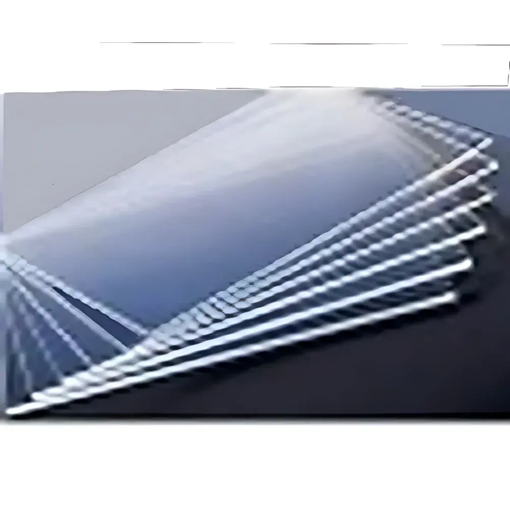
Hefei Kejing Mo-Coated Soda-Lime Glass Substrate
| Brand | Hefei Kejing |
|---|---|
| Origin | USA |
| Manufacturer Type | Authorized Distributor |
| Origin Category | Imported |
| Model | Mo-Coated Soda-Lime Glass |
| Sheet Resistance | 0.6 Ω/□ |
| Resistivity | 16 µΩ·cm |
| Mo Thickness | 500 nm (single-side sputtered) |
| Mo Crystallinity | Highly oriented polycrystalline, preferential <110> orientation |
| Surface Finish | Double-side optically polished |
| Dimensions | 100 × 100 × 1.1 mm |
| Packaging | Vacuum-sealed in Class 100 cleanroom bags, stored and shipped from Class 1000 cleanroom environment |
Overview
Molybdenum-coated soda-lime glass substrates are engineered functional materials widely employed as conductive, thermally stable, and chemically robust back contacts in thin-film photovoltaic device fabrication—particularly for CIGS (CuInGaSe₂) and CZTS (Cu₂ZnSnS₄) solar cells. This product, supplied by Hefei Kejing and manufactured in the United States, features a high-purity, highly oriented polycrystalline molybdenum film deposited via DC magnetron sputtering onto optically polished soda-lime glass. The Mo layer exhibits strong texture, which enhances adhesion to subsequent chalcogenide absorber layers and improves charge carrier collection efficiency. With a sheet resistance of 0.6 Ω/□ and bulk resistivity of 16 µΩ·cm, the substrate meets stringent requirements for low-series-resistance device architectures. Its double-side optical polish ensures compatibility with optical metrology, laser scribing, and alignment-critical thin-film deposition processes.
Key Features
- Single-side sputtered 500 nm molybdenum film with highly oriented polycrystalline structure and preferential crystallographic orientation
- Optically polished soda-lime glass substrate (both sides), enabling high-precision patterning and optical characterization
- Low sheet resistance (0.6 Ω/□) and low volume resistivity (16 µΩ·cm), optimized for photovoltaic back-contact applications
- Controlled thermal expansion coefficient matching common CIGS absorber layers, minimizing interfacial stress during annealing
- Class 1000 cleanroom handling and Class 100 cleanroom bag vacuum packaging to prevent particulate contamination and surface oxidation
- Available in three standardized geometries: 100 × 100 × 1.1 mm, 25 × 25 × 0.7 mm, and 20 × 15 × 0.7 mm—suitable for R&D prototyping and small-batch process validation
Sample Compatibility & Compliance
These Mo-coated substrates are compatible with standard thin-film processing tools including thermal evaporation, sputtering, CBD (chemical bath deposition), and rapid thermal processing (RTP) up to 550 °C in inert or reducing atmospheres. The Mo/glass interface demonstrates excellent thermal stability and minimal interdiffusion under typical CIGS co-evaporation conditions. While not certified to a specific ISO standard per se, the manufacturing and packaging protocol adheres to cleanroom practices aligned with ISO 14644-1 Class 5 (equivalent to Federal Standard 209E Class 100) for packaging and ISO 14644-1 Class 6 (Class 1000) for handling environments. Substrates are suitable for use in laboratories operating under GLP-compliant workflows where material traceability and environmental control are documented.
Software & Data Management
As a passive physical substrate, this product does not incorporate embedded electronics or firmware and therefore requires no proprietary software. However, it is fully compatible with industry-standard thin-film characterization platforms—including four-point probe systems (e.g., Keithley 2450 SourceMeter), XRD diffractometers (e.g., Rigaku SmartLab), SEM/EDS analyzers, and ellipsometers (e.g., J.A. Woollam M-2000). All dimensional and electrical specifications are provided in machine-readable format (CSV/Excel) upon request to support LIMS integration and automated QC reporting. Batch-specific certificates of conformance—including lot number, sputter date, sheet resistance map data (if measured), and packaging log—can be supplied for audit-ready documentation in regulated R&D environments.
Applications
- Back contact layer in laboratory-scale CIGS and CZTS thin-film solar cell development
- Reference substrate for evaluating Mo adhesion strength, grain growth kinetics, and interfacial reactivity during absorber layer deposition
- Platform for studying Mo oxidation behavior under controlled sulfur/selenium vapor exposure
- Calibration standard for sheet resistance mapping systems and step-height profilometers
- Substrate for flexible electronics research when paired with ultra-thin glass variants (not included in current offering)
- Baseline material in DOE (Design of Experiments) studies comparing alternative back-contact metals (e.g., Ni, Ti, W)
FAQ
Is the molybdenum layer deposited on both sides of the glass?
No—the Mo film is applied exclusively to one side. The opposite side remains bare, optically polished soda-lime glass, facilitating alignment and optical inspection.
What is the maximum recommended annealing temperature in N₂/H₂ atmosphere?
The substrate has been validated for thermal treatment up to 550 °C for ≤30 minutes in 5% H₂/N₂ without measurable Mo delamination or glass deformation.
Can these substrates be used for roll-to-roll coating processes?
Not directly—the rigid geometry and cleanroom packaging are designed for batch-based vacuum processing; flexible or continuous-web alternatives require custom engineering.
Do you provide sheet resistance uniformity maps across the coated area?
Uniformity mapping (±5% tolerance over central 80% area) is available upon request for qualification lots, but not included in standard shipment.
Is the soda-lime glass composition compliant with ASTM C162–18?
Yes—the base glass meets the compositional and optical transmittance specifications outlined in ASTM C162–18 for general-purpose flat glass used in scientific instrumentation.