InSb Crystal Substrate (合肥科晶 | Model: InSb Crystal Substrate)
| Brand | Hefei Kejing |
|---|---|
| Origin | Anhui, China |
| Manufacturer Type | Authorized Distributor |
| Origin Category | Domestic |
| Model | InSb Crystal Substrate |
| Pricing | Upon Request |
| Doping | None / Te / Ge |
| Conductivity Type | N / N / P |
| Carrier Concentration | 1–5 × 10¹⁴ cm⁻³ / 1–2 × 10¹⁵ cm⁻³ |
| Dislocation Density | < 2 × 10² cm⁻² |
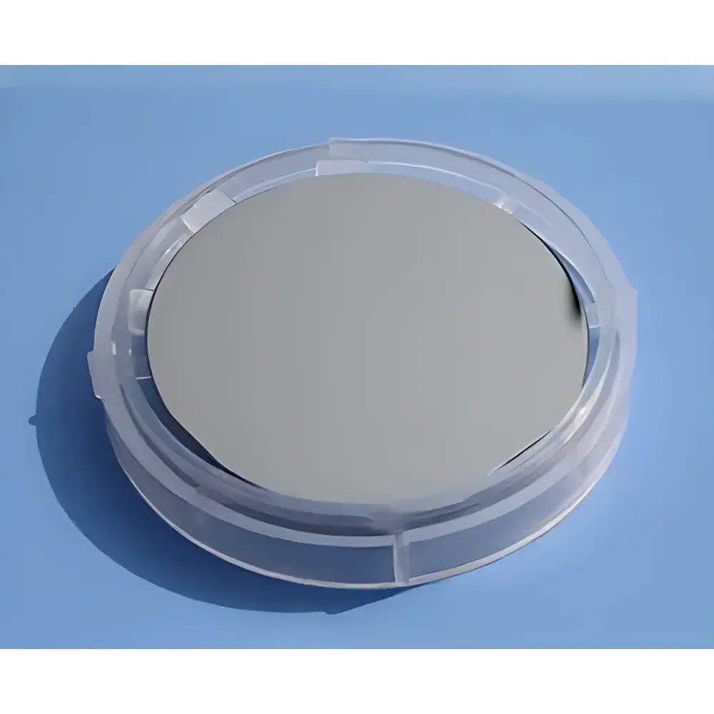
| Standard Dimensions | 2″ (50.8 mm) diameter × 0.5 mm thickness |
| Surface Roughness (Ra) | < 15 Å |
| Packaging | Class 1000 cleanroom processed |
Overview
The InSb Crystal Substrate is a high-purity, single-crystal semiconductor wafer engineered for demanding applications in infrared optoelectronics, low-temperature physics, and surface-sensitive electrochemical sensing platforms—including Quartz Crystal Microbalance (QCM) systems requiring epitaxial-grade substrates. Indium antimonide (InSb) exhibits an exceptionally narrow bandgap (~0.17 eV at 300 K), high electron mobility (>70,000 cm²/V·s at 300 K), and strong temperature-dependent resistivity—making it ideal for cryogenic Hall sensors, far-infrared detectors, and heterostructure growth via MBE or MOCVD. This substrate series is grown using the Czochralski (CZ) or Bridgman method, followed by precision lapping, polishing, and chemical-mechanical planarization (CMP) to ensure atomic-level surface integrity and crystallographic uniformity across the (111)A or (100) orientation—configurable per customer specification.
Key Features
- Single-crystal InSb wafers with controlled dopant incorporation (Te or Ge) enabling tailored carrier concentration and conductivity type (N-type or P-type)
- Low dislocation density (<2 × 10² cm⁻²) verified by molten KOH etching and X-ray topography—critical for minimizing defect-mediated leakage in thin-film device stacks
- Ultra-smooth surface finish (Ra < 15 Å) achieved through sequential colloidal silica-based CMP and megasonic cleaning—ensuring reproducible nucleation for metal/oxide thin-film deposition
- Dimensional stability under thermal cycling: coefficient of thermal expansion (CTE) matched closely to common III–V and II–VI compound semiconductors, reducing interfacial strain in heteroepitaxy
- Available in standard 2-inch (50.8 mm) diameter × 0.5 mm thickness format, with optional custom orientations ((111)A, (100), off-axis variants) and thicknesses (0.3–1.0 mm) subject to minimum order quantity
Sample Compatibility & Compliance
This substrate is compatible with standard QCM sensor head configurations (e.g., 5–10 MHz AT-cut quartz mounting fixtures), sputtering, e-beam evaporation, and atomic layer deposition (ALD) toolsets. All wafers undergo rigorous post-processing inspection per SEMI MF1390 and ASTM F1529 standards—including particle count verification (<10 particles ≥0.3 µm per cm²), surface contamination screening (FTIR and TOF-SIMS), and crystallographic orientation confirmation (XRD θ–2θ and rocking curve analysis). Packaging complies with ISO Class 5 (Class 100) cleanroom protocols, with individual wafers sealed in nitrogen-purged, static-dissipative polypropylene cassettes or laminated clean bags—fully traceable via batch-specific COA (Certificate of Analysis) including dopant profile SIMS data and surface flatness (TTV < 1.5 µm).
Software & Data Management
While the InSb substrate itself is a passive material platform, its integration into automated thin-film fabrication or QCM-based real-time monitoring workflows requires full metrology traceability. Each wafer lot ships with digital metadata aligned to SEMI E142 standards—including wafer map coordinates, doping homogeneity maps (via spreading resistance profiling), and surface roughness histograms. For GxP-regulated environments (e.g., pharmaceutical QCM biosensor development), raw inspection reports support 21 CFR Part 11-compliant electronic signatures when ingested into validated LIMS or ELN systems. Batch records are retained for ≥10 years and available upon audit request.
Applications
- Epitaxial template for InAs/InSb superlattice infrared photodetectors (MWIR/LWIR spectral bands)
- Substrate for ultra-low-noise cryogenic Hall bar structures used in quantum metrology and fundamental charge transport studies
- Functionalized surface platform in QCM-D (Quartz Crystal Microbalance with Dissipation monitoring) for real-time adsorption kinetics of biomolecules on InSb-supported Au or Pt films
- Base material for rapid thermal processing (RTP) studies investigating interdiffusion barriers in InSb/GaSb heterojunctions
- Reference standard in Raman spectroscopy calibration for phonon mode identification in narrow-gap semiconductors
FAQ
What crystallographic orientations are available?
Standard options include (111)A and (100); off-axis orientations (e.g., 2°–6° toward [110]) can be supplied with ≥4-week lead time and MOQ of 10 wafers.
Is surface orientation verification included in the COA?
Yes—each wafer lot includes XRD pole figure data confirming azimuthal alignment and mosaic spread (FWHM ≤ 0.25° for (111)A surfaces).
Can these substrates be used directly in UHV MBE chambers without additional cleaning?
They are delivered pre-baked and solvent-rinsed but require in-situ annealing (≥350°C, 10⁻⁹ Torr) prior to growth to remove residual carbon and oxide layers—standard practice for III–V substrates.
Do you provide dopant concentration profiling data?
SIMS depth profiles for Te or Ge dopants are available as an add-on service (±5% relative uncertainty, detection limit 1 × 10¹⁶ cm⁻³).
What is the maximum allowable storage humidity for long-term shelf life?
Store below 30% RH at 20–25°C in original sealed packaging; avoid exposure to ambient air >2 hours prior to processing to prevent native oxide regrowth.


")