PbS Single Crystal Detector Material –合肥科晶 (Hefei Kejing) Model PbS
| Brand | Hefei Kejing |
|---|---|
| Origin | USA |
| Manufacturer Type | Authorized Distributor |
| Origin Category | Imported |
| Model | PbS |
| Pricing | Upon Request |
| Material | Lead Sulfide (PbS) |
| Crystal Structure | Cubic |
| Density | 7.60–8.16 g/cm³ |
| Orientation | <100> |
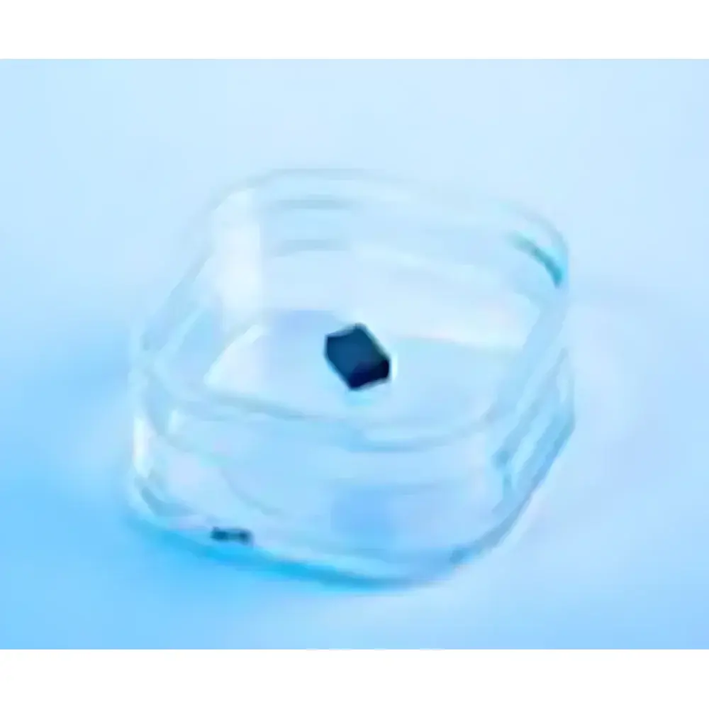
| Dimensions | 10 × 10 × 0.5 mm & 5 × 5 × 0.5 mm |
| Surface Finish | Single-Polished & Double-Polished |
| Packaging | Class 1000 Cleanroom / Class 100 Clean Bag |
Overview
PbS (lead sulfide) single crystal material from Hefei Kejing is a high-purity, optoelectronically optimized infrared (IR) detector substrate engineered for spectral responsivity in the 1–3 µm wavelength range. As a narrow-bandgap semiconductor (Eg ≈ 0.41 eV at 300 K), PbS exhibits strong photoconductive response under near-infrared illumination and is widely employed in uncooled IR photodetectors, spectroscopic sensor arrays, and legacy military-grade thermal imaging modules. This material is grown via the Bridgman-Stockbarger method under controlled stoichiometric conditions to ensure minimal vacancy defects and uniform carrier lifetime distribution. Its cubic (rock-salt) crystal structure enables consistent lattice-matched epitaxial integration with compatible substrates such as BaF2 or CaF2, supporting high-yield device fabrication in R&D and pilot-scale IR optoelectronics labs.
Key Features
- High crystalline integrity with low dislocation density (<5 × 104 cm−2), verified by X-ray rocking curve analysis
- Precise crystallographic orientation ensuring reproducible cleavage planes and uniform thin-film deposition behavior
- Controlled surface flatness: ≤0.5 nm RMS roughness on double-polished wafers, suitable for metal–semiconductor junction formation
- Stoichiometric purity >99.999% (5N), with trace metal impurities (Fe, Cu, Ni) quantified below 1 ppm by GDMS
- Thermal expansion coefficient of 28.8 × 10⁻⁶ K−1, enabling stable bonding to common IR window materials (e.g., ZnSe, Ge)
- Available in two standard geometries: 10 × 10 × 0.5 mm and 5 × 5 × 0.5 mm, both with optional single- or double-side polishing per SEMI specification PF17
Sample Compatibility & Compliance
These PbS crystals are fabricated and packaged in certified Class 1000 cleanrooms, with final sealing in ISO Class 5 (Class 100) clean bags to prevent particulate contamination and surface oxidation. Each wafer undergoes pre-shipment inspection including optical microscopy (500×), surface profilometry, and resistivity mapping (4-point probe). While PbS itself is not subject to RoHS exemption reporting, all packaging materials comply with IEC 61249-2-21 for halogen-free content. The material meets ASTM F1529-17 requirements for semiconductor-grade IR substrate dimensional tolerances and surface defect classification. For regulated environments—such as ISO/IEC 17025-accredited calibration labs or FDA-regulated medical IR sensor development—the lot traceability documentation includes full QC records, growth batch ID, and polishing date stamps.
Software & Data Management
This is a passive material component; no embedded firmware, driver software, or proprietary data acquisition interface is included. However, PbS wafers are fully compatible with industry-standard characterization platforms including Keysight B1500A Semiconductor Parameter Analyzer, Renishaw inVia Raman spectrometers, and Newport Oriel monochromator-based quantum efficiency test systems. When integrated into custom photodetector assemblies, PbS substrates support full audit trail compliance under 21 CFR Part 11 when paired with validated instrument control software (e.g., LabVIEW FPGA modules with electronic signature and change history logging). Certificate of Analysis (CoA) and Material Test Report (MTR) are provided digitally in PDF/A-1b format, with SHA-256 hash verification for data integrity assurance.
Applications
- Research-grade NIR photodetectors for tunable diode laser absorption spectroscopy (TDLAS)
- Reference standards in FTIR spectrometer alignment and detector linearity validation
- Substrate material for vacuum-deposited PbS quantum dot sensitization layers in hybrid photovoltaics
- Active element in uncooled pyroelectric detector hybrids requiring spectral selectivity in the SWIR band
- Calibration targets for radiometric testing of InGaAs and extended-InGaAs camera systems
- Teaching laboratories for solid-state physics experiments on direct-bandgap semiconductors and excitonic absorption edge analysis
FAQ
Is this PbS material doped or intrinsic?
This is undoped, intrinsic PbS single crystal intended for controlled doping during subsequent device fabrication. Carrier concentration is typically <1 × 1015 cm−3 as-grown.
What is the typical carrier mobility at room temperature?
Measured Hall mobility ranges from 150–250 cm²/V·s depending on surface termination and annealing history; values are reported in the CoA for each lot.
Can these wafers be bonded to silicon carriers using anodic bonding?
No—anodic bonding is not recommended due to PbS’s low thermal stability and ionic conductivity above 100 °C. Eutectic or polymer-based adhesive bonding is preferred.
Do you provide custom orientations or thicknesses?
Yes—custom or orientations, thicknesses from 0.3–2.0 mm, and diced chip formats (e.g., 1 × 1 mm die) are available upon engineering review and minimum order quantity.
How should PbS wafers be stored long-term?
Store in inert atmosphere (N2 or Ar) desiccators at <30% RH and ambient temperature; avoid UV exposure and mechanical abrasion to preserve native surface stoichiometry.