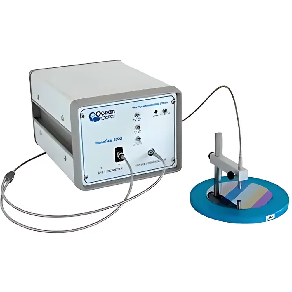
Ocean Optics NanoCalc Thin-Film Reflectance Measurement System
| Brand | Ocean Optics |
|---|---|
| Origin | USA |
| Manufacturer Type | Authorized Distributor |
| Origin Category | Imported |
| Model | NanoCalc |
| Pricing | Available Upon Request |
Overview
The Ocean Optics NanoCalc Thin-Film Reflectance Measurement System is a precision optical metrology instrument engineered for non-contact, real-time thickness characterization of thin films based on spectral reflectance analysis. It operates on the fundamental principle of interference-based optical reflectometry: incident broadband light (typically 200–1100 nm) reflects at interfaces between layers with differing refractive indices (n) and extinction coefficients (k), generating wavelength-dependent interference patterns. By fitting measured reflectance spectra to a physical multilayer optical model—solving the Fresnel equations for stratified media—the system quantifies film thickness, optical constants, and interface roughness. Designed for laboratory and industrial process environments, the NanoCalc supports rapid, high-reproducibility measurements across a broad thickness range—from 10 nm to 250 µm—with sub-nanometer resolution for single-layer films. Its compact fiber-optic architecture enables flexible integration into vacuum chambers, sputtering systems, or inline coating lines without compromising measurement fidelity.
Key Features
- Sub-nanometer thickness resolution: Achieves ≤0.1 nm repeatability for monolayer films under controlled environmental conditions.
- Multi-layer capability: Supports optical modeling and simultaneous fitting of up to three discrete layers—including substrate, interfacial layers, and top coatings—using rigorous transfer-matrix formalism.
- Fiber-coupled modular design: Integrates seamlessly with Ocean Optics’ spectrometers (e.g., QE Pro, Maya2000 Pro), tungsten-halogen and deuterium light sources, and optional motorized stages for automated mapping.
- In-situ and inline compatibility: Engineered for integration into deposition tools (PVD, CVD, ALD), etch reactors, and roll-to-roll coaters via robust optical probes with temperature-stable quartz windows and NIST-traceable calibration options.
- Real-time measurement engine: Delivers full-spectrum acquisition and model-based thickness calculation in <500 ms per point, enabling closed-loop process control and endpoint detection.
Sample Compatibility & Compliance
The NanoCalc accommodates diverse substrate and film material classes—including metallic (Al, Cu, stainless steel), dielectric (SiO₂, Si₃N₄, Al₂O₃), amorphous (photoresist, polymers), and crystalline semiconductors (Si, GaAs, sapphire). It supports both transparent and opaque substrates, provided the film exhibits measurable optical contrast. Measurement validity requires adherence to standard thin-film optical assumptions: planar, isotropic, homogeneous layers with sharp interfaces. The system complies with ISO 9277 (surface chemical analysis – ellipsometry and reflectometry), ASTM F1570 (standard guide for optical reflectance measurements of thin films), and supports audit-ready data export compliant with FDA 21 CFR Part 11 when paired with validated software configurations. All calibrations are traceable to NIST SRM 2036 (optical density standards) and certified reference films.
Software & Data Management
NanoCalc Control Software (v4.x) provides intuitive, scriptable operation via a Windows-based GUI. It includes an embedded optical constant database containing >200 experimentally verified n/k datasets (from Palik, Ioffe Institute, and peer-reviewed literature) spanning UV–NIR wavelengths. Users may import custom dispersion models (Sellmeier, Cauchy, Tauc-Lorentz), define layered stack architectures, and perform global fitting with Levenberg-Marquardt optimization. Raw spectra, fit residuals, confidence intervals, and parameter correlation matrices are exported in CSV, HDF5, and XML formats. For regulated environments, optional GxP modules enable electronic signatures, change control logs, and full audit trails meeting GLP and GMP requirements. API support (COM/.NET) allows integration with MES, SCADA, and LabVIEW-based automation frameworks.
Applications
- Process development and monitoring of SiO₂ gate oxides, Si₃N₄ passivation layers, and high-k dielectrics in semiconductor fabrication.
- In-line thickness control of anti-reflective (AR), hard-coat, and hydrophobic coatings on optical lenses, display glass, and automotive substrates.
- Quantification of photoresist thickness uniformity pre- and post-bake/etch in lithography workflows.
- Characterization of DLC (diamond-like carbon), TiN, and CrN wear-resistant coatings on tooling and medical implants.
- R&D of functional thin films—including perovskites, 2D materials (MoS₂, graphene oxide), and organic photovoltaic layers—where non-destructive, ambient-condition metrology is critical.
FAQ
What is the minimum measurable film thickness?
The NanoCalc achieves reliable quantification down to 10 nm for single-layer dielectrics on reflective substrates; sub-5 nm sensitivity is attainable for high-contrast systems (e.g., SiO₂ on Si) with optimized spectral range and signal averaging.
Can it measure films on rough or patterned substrates?
Yes—within limits. Surface roughness 5× spot size (typically ≥100 µm) preserve spectral fidelity; for nanostructured surfaces, angular-resolved or Mueller matrix extensions are recommended.
Is calibration required before each measurement?
No routine recalibration is needed; factory calibration remains stable for ≥12 months. Optional daily reference checks using certified Si/SiO₂ wafers ensure long-term drift correction.
Does the system support automated stage mapping?
Yes—via integrated USB- or Ethernet-connected motorized XY stages with programmable grid acquisition, stitching, and thickness uniformity heatmaps.
How is data integrity ensured in regulated manufacturing?
With the optional Validation Package, users receive IQ/OQ documentation, SOP templates, and 21 CFR Part 11-compliant user access controls, electronic signatures, and immutable audit logs.


