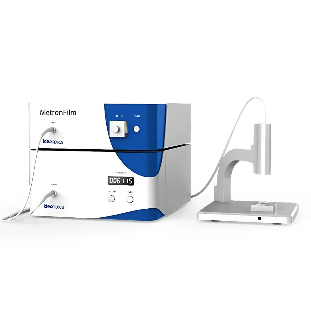
IdeaOptics MetronFilm Reflective Thin-Film Thickness Metrology System
| Brand | IdeaOptics |
|---|---|
| Origin | Shanghai, China |
| Manufacturer Type | OEM Manufacturer |
| Country of Origin | China |
| Model | MetronFilm |
| Pricing | Upon Request |
Overview
The IdeaOptics MetronFilm Reflective Thin-Film Thickness Metrology System is a non-contact, optical interference-based metrology platform engineered for high-precision, real-time characterization of thin-film thickness and complex optical constants (n and k) across single-layer and multilayer architectures. It operates on the principle of spectral reflectometry—illuminating the sample with broadband visible–NIR light (typically 350–1000 nm), capturing the intensity-modulated interference spectrum reflected from layer interfaces, and performing rigorous inverse modeling via rigorous coupled-wave analysis (RCWA) or transfer-matrix method (TMM) to extract film thicknesses and wavelength-dependent refractive index (n) and extinction coefficient (k) values. Designed for integration into R&D laboratories and high-volume manufacturing environments, the system delivers traceable, repeatable, and calibration-validated measurements without physical contact, surface damage, or vacuum requirements—making it suitable for delicate, patterned, or temperature-sensitive substrates.
Key Features
- Ultra-broad measurement range: 1 nm to 260 µm—covering atomic-scale ultrathin films (e.g., ALD-grown Al₂O₃ monolayers) through thick polymer or photoresist coatings.
- Sub-angstrom repeatability: <0.02 nm RMS thickness repeatability under controlled environmental conditions (23 ± 0.5 °C, <40% RH), validated using NIST-traceable SiO₂-on-Si reference standards.
- NIST-traceable accuracy: ±1 nm absolute accuracy for films <500 nm thick; ±0.2% relative accuracy for films ≥500 nm, certified against ISO/IEC 17025-accredited calibration protocols.
- Advanced multilayer capability: Supports full spectral fitting for up to 232 discrete layers in stacked dielectric/metal/dielectric architectures—enabling quantitative process control for 3D NAND gate-all-around stacks, tandem perovskite–silicon solar cells, and graded-index AR/HR optical coatings.
- Real-time optical constant extraction: Simultaneous determination of n(λ) and k(λ) for each layer within ≤1 second per measurement point, using proprietary dispersion-aware fitting algorithms trained on >10⁴ experimentally verified material optical databases.
Sample Compatibility & Compliance
The MetronFilm system accommodates rigid and flexible substrates including silicon wafers (up to 300 mm diameter), fused silica, BK7 glass, PET, PI, sapphire, and GaN-on-silicon heterostructures. It supports flat, slightly curved (radius >500 mm), and patterned surfaces with feature sizes down to 5 µm (no spatial averaging artifacts). All hardware and firmware comply with CE marking requirements (EMC Directive 2014/30/EU, Low Voltage Directive 2014/35/EU) and meet RoHS 2011/65/EU substance restrictions. Software architecture adheres to FDA 21 CFR Part 11 principles—including electronic signature enforcement, audit trail logging (with immutable timestamps and user attribution), and role-based access control—supporting GLP and GMP-regulated environments in semiconductor, photovoltaic, and medical optics manufacturing.
Software & Data Management
The bundled MetronStudio™ software provides a modular, scriptable interface for measurement setup, model definition, spectral fitting, and statistical reporting. It includes preconfigured templates for common applications (e.g., “SiNₓ on c-Si – PERC passivation”, “TiO₂/ZrO₂ AR stack on CR-39 lens substrate”) and supports custom layer stack import via XML or CSV. Raw spectra, fitted models, residuals, and confidence intervals are stored in HDF5 format with embedded metadata (instrument ID, calibration date, operator ID, ambient conditions). Export options include CSV, PDF reports (with ISO/IEC 17025-compliant uncertainty budgets), and direct integration with MES/SPC systems via OPC UA or RESTful API. Firmware updates and spectral library revisions are delivered through secure, digitally signed channels compliant with IEC 62443-3-3.
Applications
- Semiconductor front-end process control: In-line monitoring of high-k dielectrics (HfO₂, Al₂O₃), interfacial oxides, and epitaxial layers in logic and memory fabrication—especially critical for 3D NAND staircase etch verification and gate-last integration.
- Optical coating QC: Quantitative validation of multi-functional AR+HC stacks on ophthalmic lenses, camera modules, and laser optics—ensuring target n/k dispersion profiles and thickness uniformity across 200 mm substrates.
- Photovoltaic R&D and production: In-process characterization of SiNₓ antireflection layers, Al₂O₃ passivation films, and ITO/Ag/ITO transparent electrodes in PERC, TOPCon, and heterojunction solar cells.
- Flexible electronics: Thickness and optical homogeneity mapping of transparent conductive oxides (TCOs), organic semiconductors (e.g., P3HT:PCBM), and barrier layers on roll-to-roll coated PET or PI foils.
- Academic materials research: In situ growth monitoring of thin films during sputtering, evaporation, or ALD—enabled by optional fiber-coupled probe head integration.
FAQ
Does the MetronFilm system require vacuum or inert atmosphere for operation?
No—it operates under ambient laboratory conditions and is optimized for air-based reflectance measurements. Optional purge enclosures are available for moisture-sensitive samples.
Can it measure films on rough or textured substrates?
Yes—within limits. Surface roughness RMS 1 µm are recommended for reliable fitting; scattering corrections can be applied for moderate texturing (e.g., pyramidal Si textures in solar cells).
Is the system compatible with automated wafer handling or robotic integration?
Yes—equipped with SECS/GEM-compliant communication protocol support and mechanical interface plates for integration into cluster tools or inline metrology stations.
How frequently does the system require recalibration?
Annual NIST-traceable calibration is recommended; drift monitoring is performed automatically using built-in reference channels and daily verification routines with certified standards.
What spectral resolution and SNR specifications does the integrated spectrometer provide?
The custom-designed Czerny–Turner spectrometer delivers 1000:1 SNR (at 50 ms integration time), optimized for interference fringe contrast detection across the full 350–1000 nm range.


