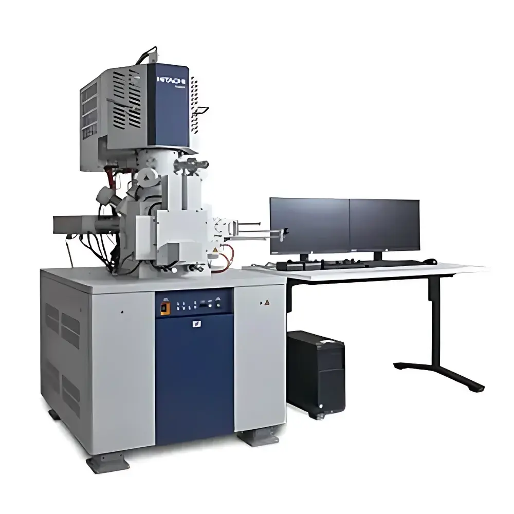
Hitachi SU8600 Cold Field-Emission Scanning Electron Microscope
| Brand | Hitachi |
|---|---|
| Origin | Japan |
| Manufacturer | Hitachi High-Tech Corporation |
| Type | Floor-standing FE-SEM |
| Electron Source | Cold Field-Emission Gun |
| Secondary Electron Resolution | 0.6 nm @ 15 kV |
| Magnification Range | 20× – 2,000,000× |
| Accelerating Voltage | 0.5–30 kV (standard mode) |
| Backscattered Electron Resolution | Not specified |
Overview
The Hitachi SU8600 is a high-performance cold field-emission scanning electron microscope (FE-SEM) engineered for nanoscale imaging, compositional analysis, and structural characterization in demanding R&D and industrial quality control environments. Operating on the fundamental principle of raster-scanned electron beam interaction with solid specimens, the SU8600 generates high-fidelity signals—including secondary electrons (SE), backscattered electrons (BSE), cathodoluminescence (CL), and characteristic X-rays—enabling simultaneous topographic, crystallographic, and elemental information extraction. Its cold field-emission electron source delivers exceptional brightness, energy stability, and probe coherence, supporting sub-nanometer resolution imaging at low accelerating voltages—a critical capability for beam-sensitive materials such as polymers, biological coatings, and soft nanocomposites. Designed as a floor-standing platform, the SU8600 integrates robust mechanical stability, ultra-high vacuum architecture (<1.0 × 10⁻⁷ Pa), and active vibration/EMI isolation to ensure long-term imaging reproducibility and analytical repeatability across multi-hour acquisition sessions.
Key Features
- Cold field-emission electron gun with <1.0 nm probe size at 1 kV, enabling high-resolution surface imaging without conductive coating for non-conductive or beam-sensitive specimens.
- Automated column alignment and focus/stigmation routines reduce operator dependency and minimize inter-user variability in image quality and measurement consistency.
- Multi-detector signal acquisition: Up to six detectors—including in-lens SE, through-the-lens BSE, annular BSE, STEM-in-SEM, CL, and EDS—can be simultaneously enabled and synchronized for correlative data capture.
- Ultra-high pixel density imaging: Optional 40,960 × 30,720 pixel acquisition (1.25 billion pixels per frame), delivering 64× greater spatial coverage than previous-generation Hitachi FE-SEMs—ideal for statistical microstructural analysis and defect mapping across mm-scale regions.
- Enhanced BSE detection speed and signal-to-noise ratio via newly developed high-efficiency scintillator-photomultiplier assemblies, improving Z-contrast fidelity and phase discrimination in multiphase alloys and heterogeneous catalysts.
- Integrated stage with ±70° tilt, 360° rotation, and 100 mm X-Y travel supports comprehensive 3D reconstruction, cross-sectional imaging, and site-specific analysis under variable geometry conditions.
Sample Compatibility & Compliance
The SU8600 accommodates standard 100 mm diameter stub-mounted samples up to 50 mm height, with optional holders for cryo-transfer, heating (up to 800 °C), or electrical biasing. Its low-voltage imaging capability (down to 0.5 kV) significantly reduces charging artifacts and beam damage in insulating or organic materials—making it suitable for applications aligned with ISO 13782 (electron microscopy of polymers), ASTM E1558 (SEM specimen preparation), and USP (microstructural evaluation of pharmaceutical particulates). The system’s hardware and software architecture comply with GLP and GMP documentation requirements, including audit-trail-enabled user logins, parameter change logging, and instrument calibration history tracking—supporting regulatory submissions under FDA 21 CFR Part 11 when paired with validated EM Flow Creator workflows.
Software & Data Management
Hitachi’s proprietary SEM Control Software provides intuitive, workflow-driven operation—from automated landing voltage optimization and contrast/brightness normalization to batch-acquisition scripting. The optional EM Flow Creator module enables fully customizable, condition-based automation: users define trigger logic (e.g., stage position, detector threshold, or EDS count rate), then schedule sequential image capture, EDS mapping, or line-scan acquisitions across hundreds of fields-of-view without manual intervention. All acquired data—including raw TIFF stacks, metadata-rich .hdf5 files, and EDS spectra—are stored with embedded acquisition parameters, instrument state logs, and user annotations. Native support for open formats (e.g., TIFF, MRC, EMDB-compatible HDF5) ensures compatibility with third-party quantification platforms such as DigitalMicrograph, HyperSpy, and Python-based image analysis pipelines.
Applications
The SU8600 serves as a primary analytical tool in semiconductor process development (e.g., gate oxide thickness verification, trench profile metrology), advanced battery electrode microstructure assessment (NMC, Si-anode porosity and crack propagation), metallurgical phase identification in aerospace superalloys, nanofiber morphology characterization for filtration membranes, and subcellular organelle visualization in freeze-fractured biological tissues. Its high-throughput, multi-signal acquisition capability directly supports materials informatics initiatives—feeding structured datasets into machine learning models for predictive microstructure–property relationships. In failure analysis labs, the combination of high-resolution low-kV SE imaging and fast BSE phase mapping accelerates root-cause identification in solder joint voiding, die attach delamination, and interconnect electromigration.
FAQ
What vacuum level does the SU8600 achieve in the specimen chamber?
The main chamber maintains a base pressure of ≤1.0 × 10⁻⁷ Pa using a combination of turbomolecular and ion pumps—essential for stable cold FEG operation and minimizing hydrocarbon contamination during extended imaging.
Is the SU8600 compatible with energy-dispersive X-ray spectroscopy (EDS)?
Yes—the system features standardized EDS port interfaces and integrated stage synchronization for automated WDS/EDS mapping; compatible with Oxford Instruments X-MaxN, Thermo Scientific SuperATM, and Bruker QUANTAX detectors.
Can the SU8600 perform automated particle analysis?
When configured with EM Flow Creator and optional particle recognition plugins, it executes fully autonomous particle detection, classification, and size/shape distribution reporting across large-area montages—aligned with ISO 13322-2 and ASTM E1245 standards.
Does the system support in situ electrical biasing or heating experiments?
Yes—via Hitachi’s modular stage options, including the NanoHeat™ heating stage (RT–800 °C) and the NanoBias™ 4-probe electrical characterization holder, both with real-time current/voltage monitoring and thermal drift compensation.
How is instrument calibration traceability maintained?
All geometric calibrations (magnification, stage movement, tilt angle) are performed using NIST-traceable grating standards; calibration certificates and validation reports are generated within the software and archived with each session’s metadata.


